Transparent conductive film, method for production thereof and touch panel therewith

Active Publication Date: 2008-07-24
NITTO DENKO CORP
View PDF18 Cites 91 Cited by
  • Summary
  • Abstract
  • Description
  • Claims
  • Application Information

AI Technical Summary

Benefits of technology

[0024]In conventional transparent conductive films, patterned transparent conductor layers produce a clear difference in reflectance between the patterned and non-patterned portions so that the appearance can be degraded. In the transparent conductive film of the present invention, the transparent conductor layer is patterned, but the non-patterned portion has the undercoat layer so that the difference in reflectance between the patterned and non-patterned portions can be kept small. Thus, the defect caused by patterned portions distinguishable from one another can be avoided so that a good appearance can be provided. The f

Problems solved by technology

When the transparent conductor layer is patterned, however, the difference between the patterned portion and th

Method used


Image

  • Transparent conductive film, method for production thereof and touch panel therewith
  • Transparent conductive film, method for production thereof and touch panel therewith
  • Transparent conductive film, method for production thereof and touch panel therewith

Examples


example 1

Formation of Undercoat Layer

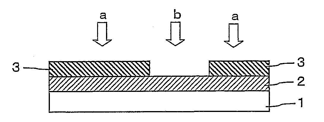
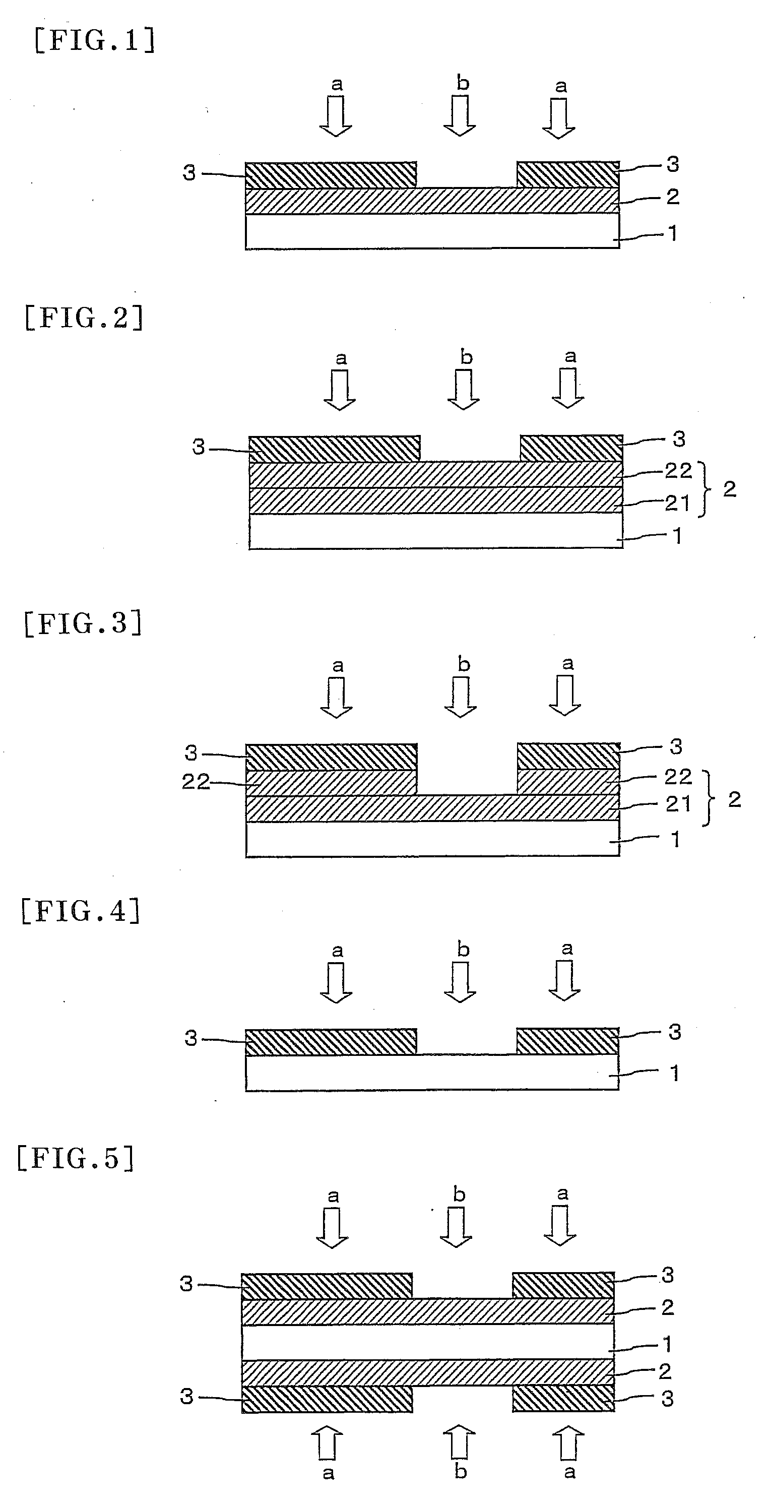
[0100]A 185 nm-thick first undercoat layer was formed from a thermosetting resin (light refractive index n of 1.54) on one side of a film substrate composed of a 25 μm-thick polyethylene terephthalate film (hereinafter referred to as “PET film”). The thermosetting resin was composed of a melamine resin, an alkyd resin and an organosilane:condensate (2:2:1 in weight ratio). A silica sol (Colcoat P manufactured by Colcoat Co., Ltd.) was then diluted with ethanol to a solids content concentration of 2%. The diluted silica sol was applied to the first undercoat layer by a silica coating method and then dried and cured at 150° C. for 2 minutes to form a 33 nm-thick second undercoat layer (a SiO2 film with a light refractive index of 1.46). Both of the first and second undercoat layers formed had a surface resistance of 1×10¹² Ω / square or more.

(Formation of Transparent Conductor Layer)

[0101]A 22 nm-thick ITO film (with a light refractive index of 2.00) of an in...

example 2

[0108]A transparent laminated conductive film with a patterned ITO film was prepared using the process of Example 1, except that the patterning of the second undercoat layer by etching was not performed.

example 3

[0109]A transparent laminated conductive film with a patterned ITO film was prepared using the process of Example 1, except that the thickness of the first undercoat layer was changed to 35 nm and that the second undercoat layer was not formed.


PUM

PropertyMeasurementUnit
Thicknessaaaaaaaaaa
Thicknessaaaaaaaaaa
Nanoscale particle sizeaaaaaaaaaa

Abstract

A transparent conductive film includes: a transparent film substrate; a transparent conductor layer provided on one or both sides of the transparent film substrate; and at least one undercoat layer interposed between the transparent film substrate and the transparent conductor layer; wherein: the transparent conductor layer is patterned; and a non-patterned portion not having the transparent conductor layer has the at least one undercoat layer.

Description

BACKGROUND OF THE INVENTION[0001]1. Field of the Invention[0002]The present invention relates to a transparent conductive film that has transparency in the visible light range and includes a film substrate and a transparent conductor layer provided on the substrate with an undercoat layer interposed therebetween, and also to a method for production thereof. The invention also relates to a touch panel including the transparent conductive film.[0003]The transparent conductive film of the present invention may be used for transparent electrodes in touch panels and display systems such as liquid crystal displays and electroluminescence displays and also used for electromagnetic wave shielding or prevention of static charge of transparent products. In particular, the transparent conductive film of the present invention is preferably used for touch panels. The transparent conductive film of the invention is particularly suitable for use in capacitive coupling type touch panels.[0004]2. De...

Claims


Application Information

Patent Timeline
IPC IPC(8): B32B3/30B44C1/22
CPCG06F3/044G06F3/04886H01H2201/028H01H2209/082Y10T428/24802H01H2229/016H01H2239/006Y10T428/24612H01H2219/012B32B27/06B32B33/00G06F2203/04103H01B5/14
Inventor NASHIKI, TOMOTAKESUGAWARA, HIDEO
Owner NITTO DENKO CORP
Why Eureka
Try Eureka