Atomic layer deposition system including a plurality of exhaust tubes

a technology of atomic layer and exhaust tube, which is applied in the direction of liquid surface applicators, chemical vapor deposition coatings, coatings, etc., can solve the problems of difficult to form capacitor insulation films, and increasing the size of semiconductor wafers, etc., to achieve uniform film quality, improve coating performance of resultant films, and improve the effect of aspect ratio

Inactive Publication Date: 2008-07-24
PS4 LUXCO SARL
View PDF6 Cites 401 Cited by
  • Summary
  • Abstract
  • Description
  • Claims
  • Application Information

AI Technical Summary

Benefits of technology

[0016]It is therefore an object of the present invention to provide an ALD system in which the coating performance of the resultant film can be improved by controlling the gas flow in each step of gas introduction, withou...

Problems solved by technology

In this background, it has become difficult to form a capacitor insulation film having an excellent coating performance while using the conventional CVD (Chemical Vapor Deposition) technique.
On the other hand, in the semiconductor device industry, the price fluctuation is extensive and ceaseless.
In such circumstances, a trend of increasing the size of a semiconductor wafer has been accelerated, whereas formation of a uniform film in the whole area of the semiconductor wafer has become difficult along with the development of the large-size semiconductor wafer.
This may cause the problem that those films cannot be formed uniformly in the whole area of the semiconductor wafer.
Further, in the circumstances in which the tendency of high-aspect-ratio structure is being accelerated for the capacitor insulation film as described above, even if the film thickness and quality are uniform in the upper portion, for example, of the cylindrical hole, the film thickness and quality in the lower portion of the cylindrical ...

Method used


Image

  • Atomic layer deposition system including a plurality of exhaust tubes
  • Atomic layer deposition system including a plurality of exhaust tubes
  • Atomic layer deposition system including a plurality of exhaust tubes

Examples


first embodiment

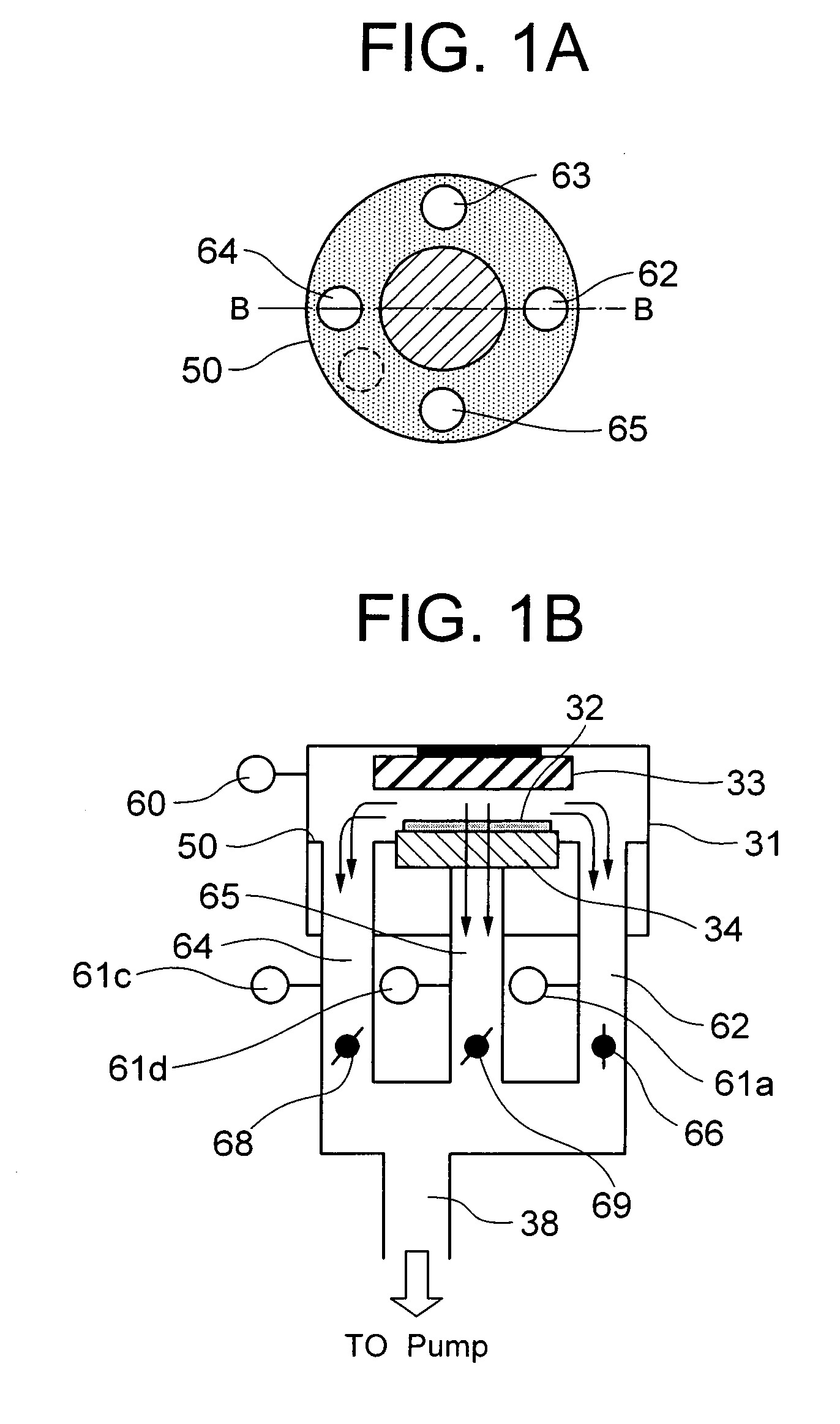
[0034]FIGS. 1A and 1B show an ALD system of use in a semiconductor manufacturing system according to a first embodiment of the present invention. FIG 1A is a top plan view of the ALD system, and FIG 1B is a sectional view taken along line B-B shown in FIG 1A. The semiconductor manufacturing system of the present embodiment includes an in-line ALD system which can form a capacitor insulation film by controlling the introduced gas to uniformly flow over the entire area of the semiconductor wafer under substantially all of the filming conditions. The structure of the in-line ALD system will be described first, and thereafter a process for forming the capacitor insulation film by using the ALD system will be described.

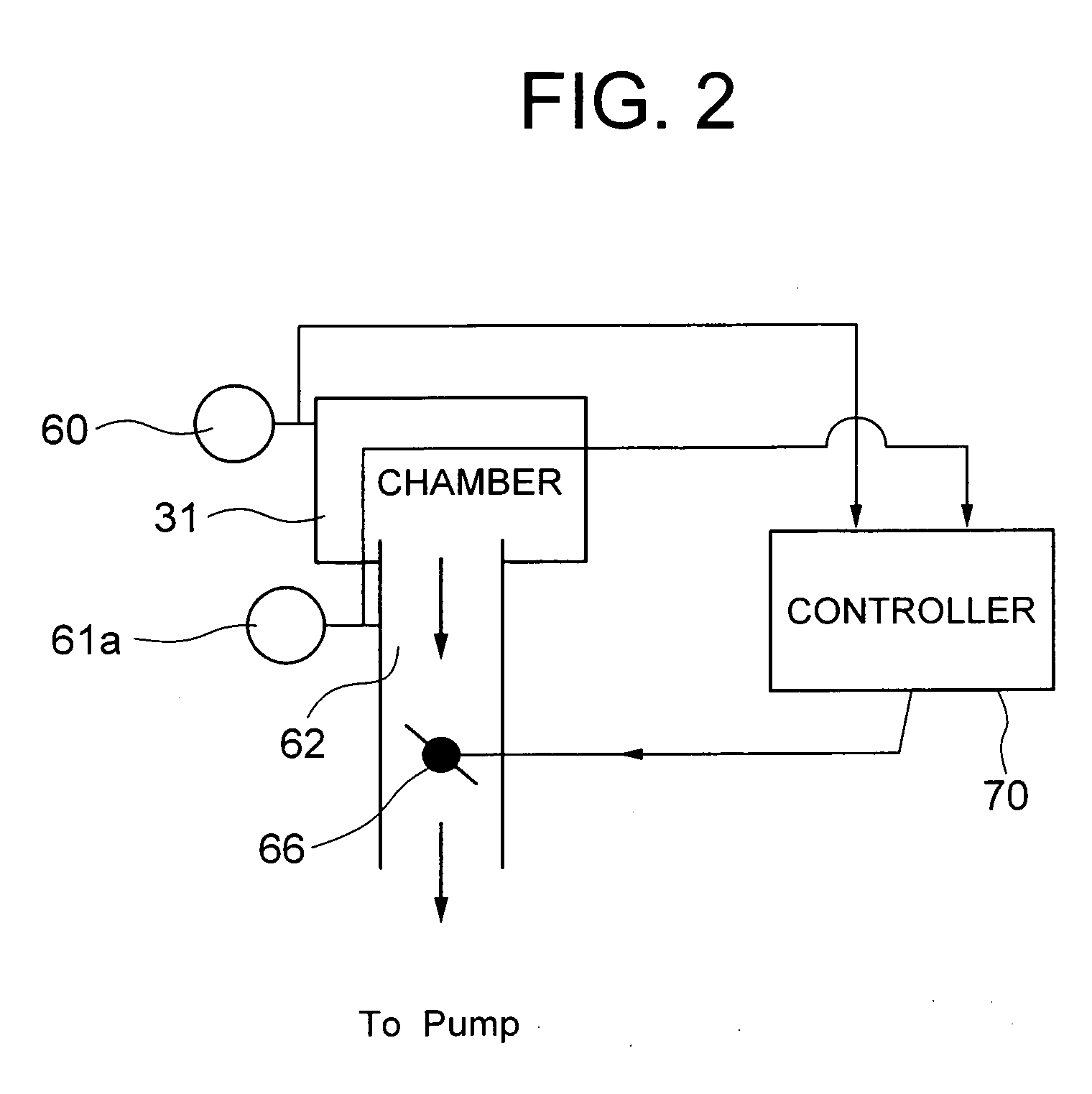
[0035]The ALD system in the present embodiment includes a shield plate 10 including at least two (four in the example of FIG. 1) exhaust tubes 62 to 65 extending from the shield plate 50 and having a substantially equal diameter. The exhaust tubes 62 to 65 include therein ...

second embodiment

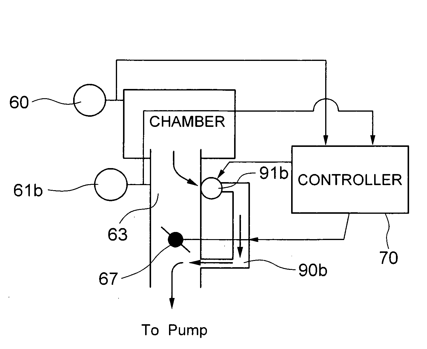
[0046]FIGS. 6A and 6B show a top plan view and a sectional view, respectively, of an ALD system in a semiconductor manufacturing system according to a second embodiment of the present invention. FIG. 6B is taken along line B-B shown in FIG. 6A. The configuration of the second embodiment is similar to that of the first embodiment in that a plurality of exhaust tubes 62 to 65 are communicated with the reaction chamber, and the exhaust tubes 62 to 65 include therein the vacuum gauges 61a to 61d, respectively, for adjusting exhaust volume of the exhaust tubes and the pressure-control rotary valves 66 to 69, respectively. The second embodiment is different from the first embodiment in that bypass lines 90a to 90d bypassing the pressure-control rotary valves 66 to 69, respectively, are further provided. Isolation valves 91a to 91d are attached to the bypass lines 90a to 90, respectively. The opening / closing posture of the isolation valves 91a to 91d provides a function similar to that of ...


PUM

PropertyMeasurementUnit
Angleaaaaaaaaaa
Pressureaaaaaaaaaa
Angleaaaaaaaaaa

Abstract

An atomic layer deposition system includes a reaction chamber, a plurality of exhaust tubes communicated to the reaction chamber, a plurality of first vacuum gauges for monitoring the degree of vacuum of the respective exhaust tubes, a second vacuum gauge for monitoring the degree of vacuum of the reaction chamber, and control valves for adjusting the exhaust volume of the exhaust tubes independently of one another. The control valves are controlled based on the pressures measured by the first and second control valves for achieving a uniform flow of the vapor phase reactant.

Description

[0001]This application is based upon and claims the benefit of priority from Japanese patent application No. 2007-011784, the disclosure of which is incorporated herein in its entirety by reference.BACKGROUND OF THE INVENTION[0002]1. Field of the Invention[0003]The present invention relates to an atomic layer deposition (ALD) system and a method of depositing an insulation film by using an ALD process, and more particularly, to an improvement of the process of depositing the insulation film in the semiconductor device by using an ALD technique.[0004]2. Description of the Related Art[0005]With the improvement of micro-fabrication technology, development of a higher integration density of DRAM devices has been accelerated, to achieve a reduction in the occupied area for cell capacitors in the DRAM device. On the other hand, it is necessary to maintain the capacitance of the capacitors required for operating the DRAM devices. This resulted in the main stream of capacitors having a cyli...

Claims


Application Information

Patent Timeline
IPC IPC(8): H01L21/31B05C11/00
CPCC23C16/45527C23C16/4412
Inventor KOMEDA, KENJI
Owner PS4 LUXCO SARL
Why Eureka
Try Eureka