Silicon Deflector on a Silicon Submount For Light Emitting Diodes

a technology of light-emitting diodes and silicon deflectors, which is applied in the direction of mountings, optical elements, instruments, etc., can solve the problems of affecting the quality of light e affecting the effect of light emitted towards the mounting surface or to the side, and affecting the quality of light emitted, so as to achieve high reflection quality

Inactive Publication Date: 2008-07-31
KONINKLIJKE PHILIPS ELECTRONICS NV
View PDF8 Cites 16 Cited by
  • Summary
  • Abstract
  • Description
  • Claims
  • Application Information

AI Technical Summary

Benefits of technology

[0011]This is especially advantageous due to the fact that the process of wet etching is scalable to a large extent and does not rely on power-consuming plasma ovens to operate.

Problems solved by technology

Due to the light emitting characteristics of the LEDs however, some of the light that is emitted towards the mounting surface or to the side gets absorbed in the neighbouring LEDs.
This light is lost and cannot be directed to the front.
However, there still exist significant drawbacks in the state of the art as described above.
One key element of this optical illumination system, the shaped metallic reflecting bins, is difficult to fabricate.
Especially in the case of a silicon substrate, the process of reactive ion etching, being a plasma etching process and thus a dry process, is uneconomical due to the limited capacity of plasma etchers, it has a high energy requirement and it is difficult to control with respect to the formation of fine structures upon the substrate.

Method used


Image

  • Silicon Deflector on a Silicon Submount For Light Emitting Diodes
  • Silicon Deflector on a Silicon Submount For Light Emitting Diodes
  • Silicon Deflector on a Silicon Submount For Light Emitting Diodes

Examples


Embodiment Construction

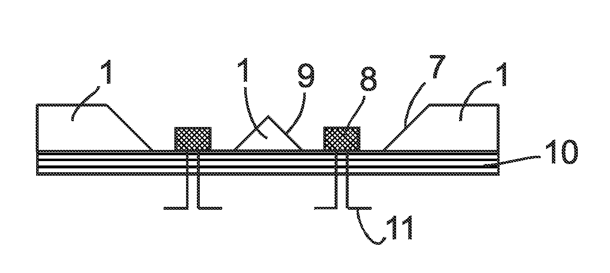
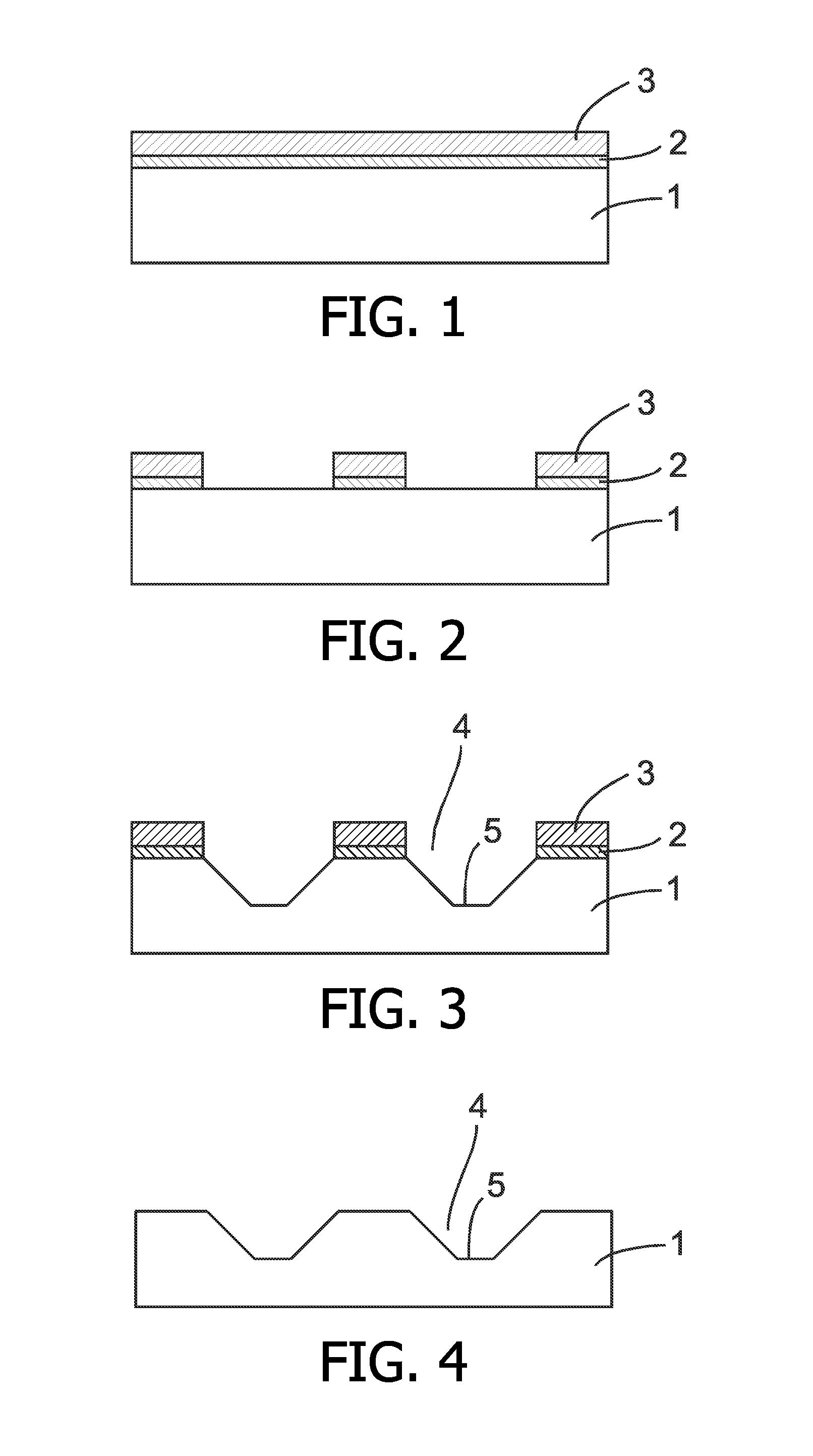
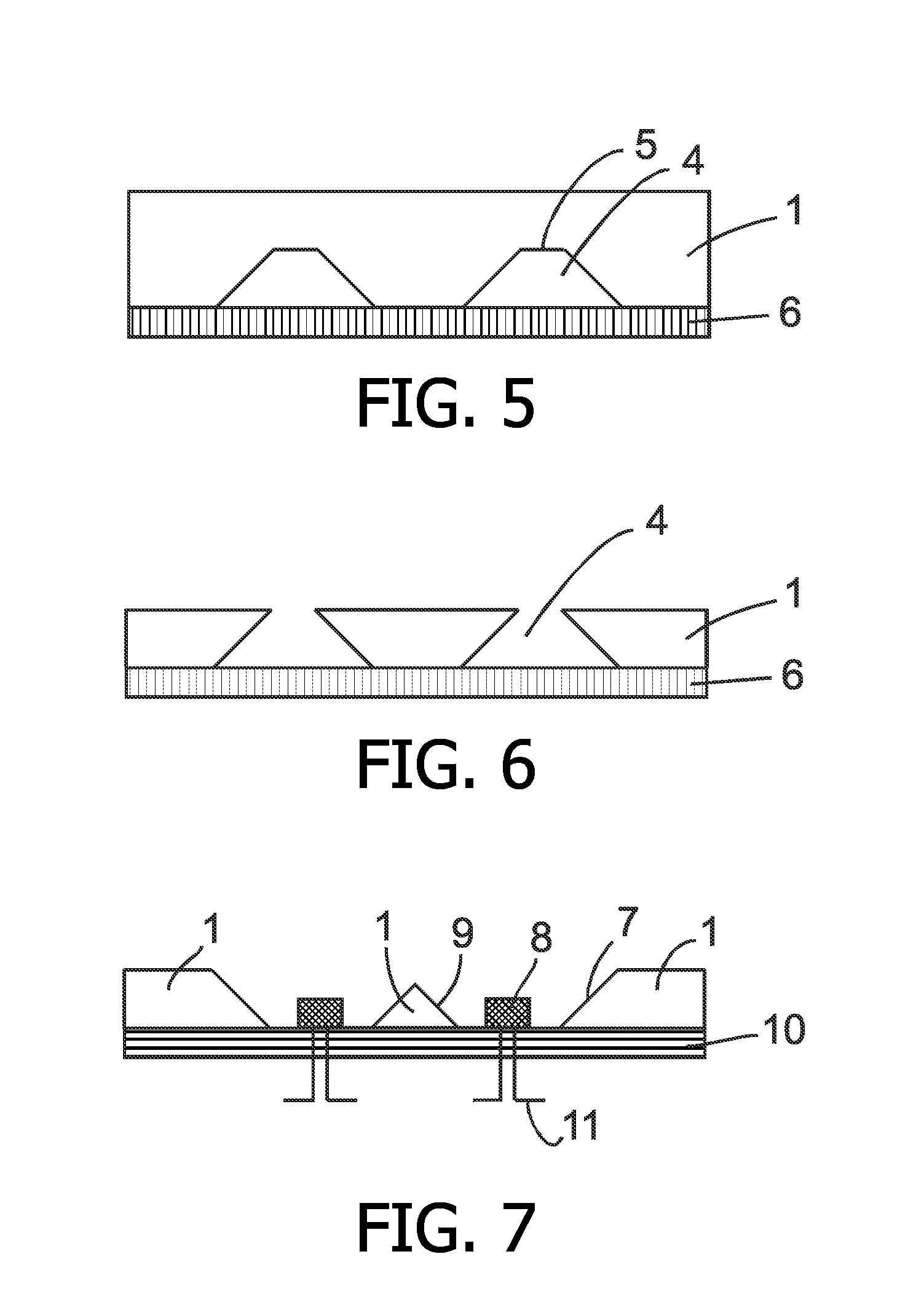
[0031]In one embodiment of the present invention, the silicon material is wet etched to such an extent that a through-going opening is etched into the material. This has the advantage that the grinding step (FIG. 6) can be shortened or omitted. Alternatively, in another embodiment of the present invention, the silicon material is wet etched to such an extent that a cavity with a bottom is formed in the material. This has the advantage that the silicon material does not need to be immersed into the wet etching solution for a long time. Depending on the nature of the etchant, finer structures may be etched into the material in a shorter period of time. The back side of the silicon substrate is then subjected to grinding (as shown in FIG. 6).

[0032]In a preferred embodiment of the present invention, the process for the manufacturing of reflecting optical barriers comprising silicon according to the present invention comprises the following steps: grinding the silicon wafer to a given th...


PUM

PropertyMeasurementUnit
heightaaaaaaaaaa
heightaaaaaaaaaa
heightaaaaaaaaaa

Abstract

The present invention deals with a process for the manufacturing of reflecting optical barriers comprising silicon and useful in combination with light emitting devices, wherein the process comprises anisotropic wet etching of the silicon material in such a manner that the rate of etching along the crystallographic (111) plane of the silicon material is slower than the rate of etching along the (110) and (100) planes. The present invention further comprises a reflecting optical barrier useful in combination with light emitting devices and a system containing at least one light emitting device comprising a reflecting optical barrier.

Description

FIELD OF THE INVENTION[0001]The present invention is directed to a process for the manufacturing of reflecting optical barriers. In particular, the present invention is directed to a process for the manufacturing of reflecting optical barriers comprising silicon useful in the production of light emitting devices.BACKGROUND OF THE INVENTION[0002]The large-volume application of high brightness light emitting diodes (LEDs) is well established for signalling and signage. They are expected to replace conventional lamps in lighting applications within a few years.[0003]One of the interesting features of LEDs is the colour purity of the LED devices. This can be used in lamps with programmable beam colour. For multicolour LED lamps a number of LEDs with different colours need to be mounted in low distance of each other to make small light mixing optics possible.[0004]A known principle to achieve a compact multi-chip module is to use naked LED chips mounted on a common substrate.[0005]Due to...

Claims


Application Information

Patent Timeline
Patent Type & Authority Applications(United States)
IPC IPC(8): H01L33/00C23F1/00G02B7/182H01L33/60H01L33/62
CPCG02B1/02G02B27/0977H01L33/60H01L33/62H01L2924/0002H01L2924/00
Inventor WENDT, MATTHIASFERRU, GILLES
Owner KONINKLIJKE PHILIPS ELECTRONICS NV
Why Eureka
Try Eureka