Semiconductor apparatus

a technology of semiconductor devices and semiconductors, applied in the direction of semiconductor devices, electrical devices, basic electric elements, etc., can solve the problems of low device breakdown voltage, and low breakdown voltage of the termination region

Inactive Publication Date: 2008-07-31
KK TOSHIBA
View PDF11 Cites 71 Cited by
  • Summary
  • Abstract
  • Description
  • Claims
  • Application Information

AI Technical Summary

Problems solved by technology

Thus there is a tradeoff between the device breakdown voltage and the ON resistance.
Thus the breakdown voltage of the termination region is likely to decrease.
On the other hand, the depletion layer does not easily extend into the drift layer outside the field plate electrode.
Hence the electric field directly below the edge of the field plate electrode unfortunately increases.
However, if the insulating film is formed thick, the substrate is likely to warp due to the difference in thermal expansion coefficient as compared with the semiconductor layer (silicon).
Thus it is currently difficult to realize a termination structure that is supposed to exhibit a high breakdown voltage in principle.

Method used


Image

  • Semiconductor apparatus
  • Semiconductor apparatus
  • Semiconductor apparatus

Examples


first embodiment

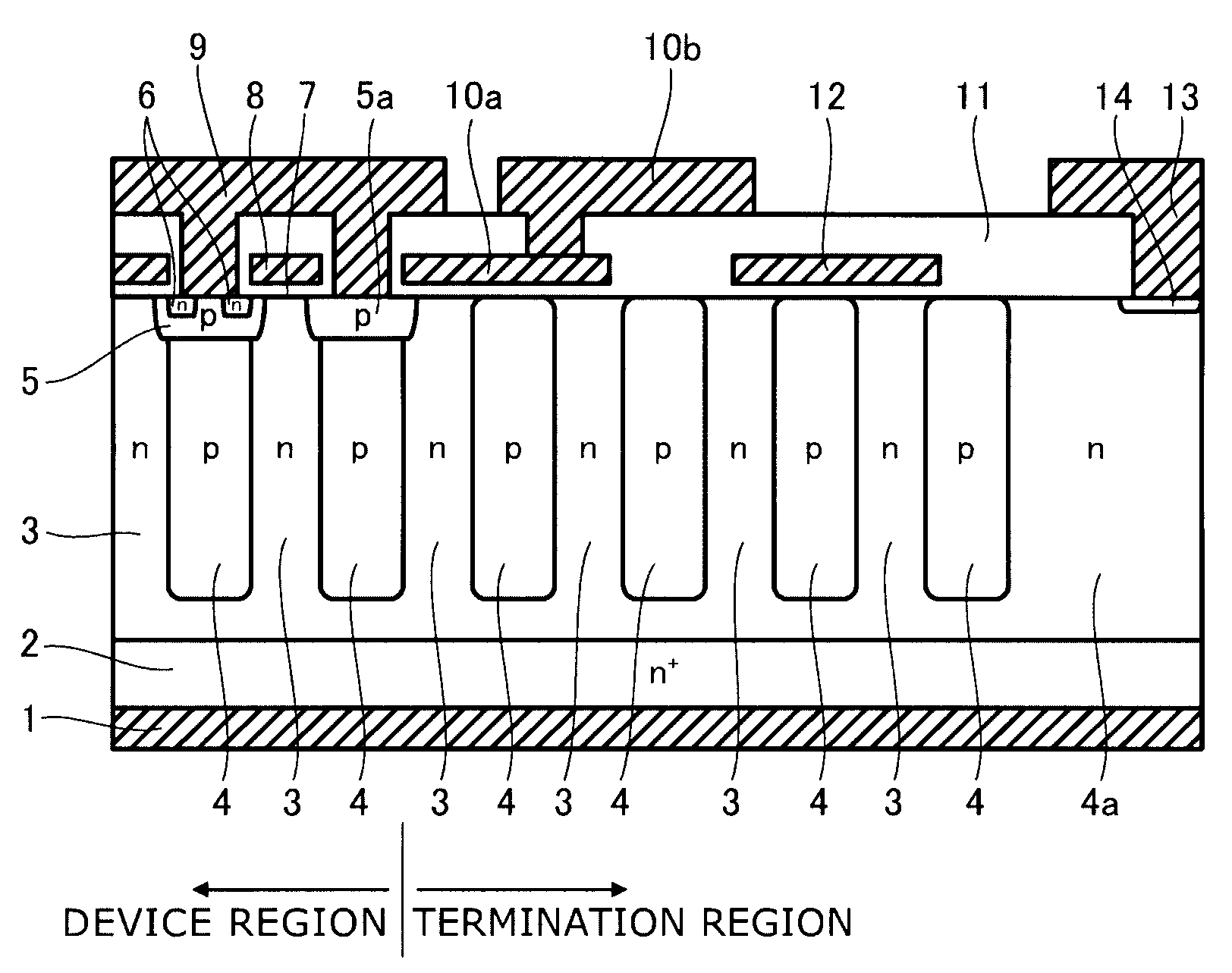
[0021]FIG. 1 is a cross-sectional view schematically showing the configuration of a semiconductor apparatus according to a first embodiment of the invention.

[0022]The semiconductor apparatus according to this embodiment is a vertical device in which a main current path is formed in the vertical direction (the direction generally perpendicular to the major surface of the semiconductor layer) connecting between a first main electrode and a second main electrode provided on the frontside and the backside of the semiconductor layer, respectively. The semiconductor apparatus according to this embodiment comprises a device region in which the main current path is formed and a termination region surrounding outside the device region.

[0023]On the major surface of a drain layer 2 serving as a first first-conductivity-type semiconductor layer of n+-type silicon having a high impurity concentration, n-type pillar layers 3 of n-type silicon serving as second first-conductivity-type semiconducto...

second embodiment

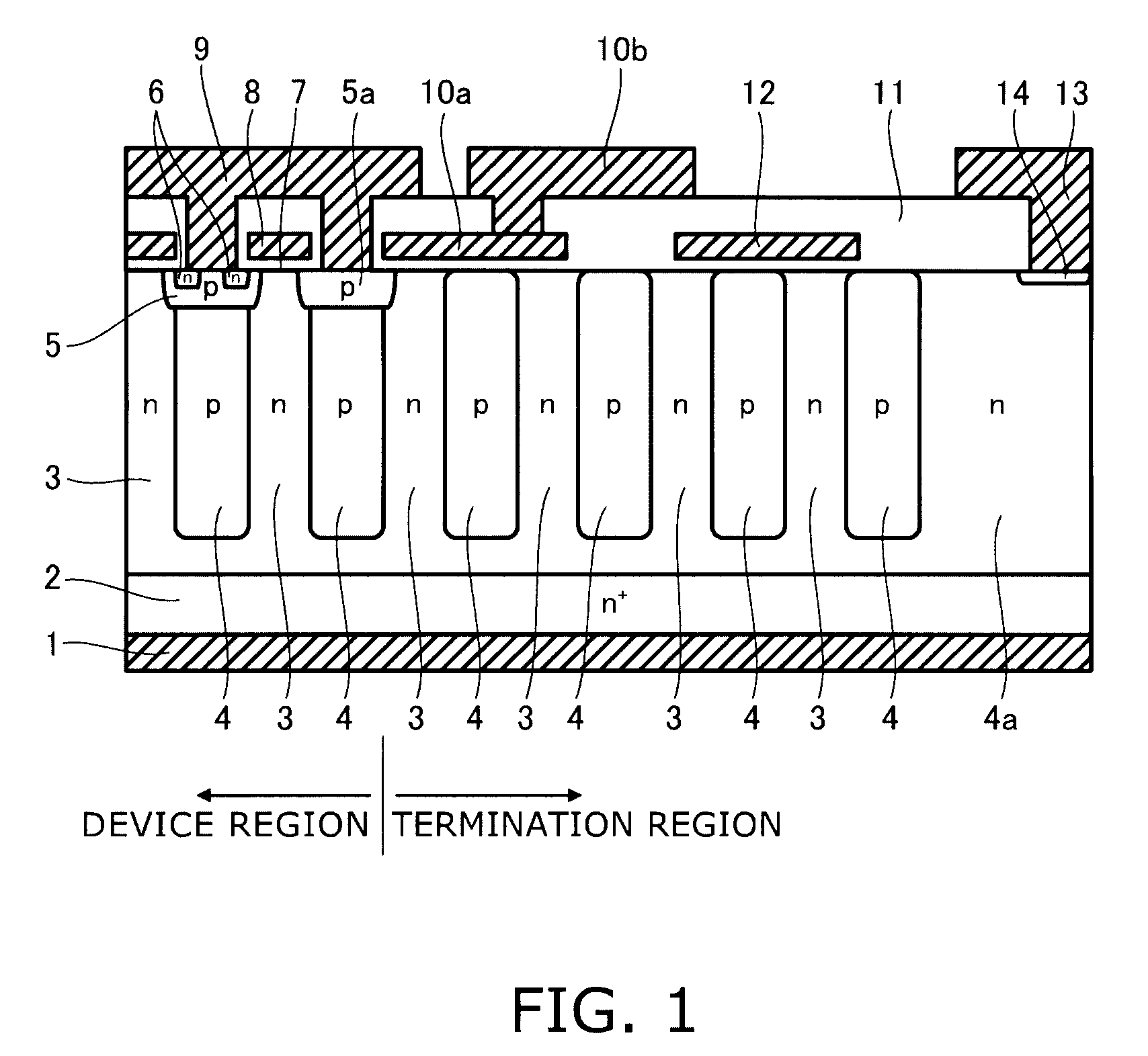
[0046]FIG. 5 is a cross-sectional view schematically showing the configuration of a semiconductor apparatus according to a second embodiment of the invention.

[0047]In this embodiment, on the field insulating film 11 outside the field plate electrodes 10a, 10b, a plurality of (two, in the example shown) floating field plate electrodes 12b, 12c spaced from each other are provided. The inner edge of the floating field plate electrode (second filed plate electrode) 12b overlies the outer edge of the field plate electrode 10b through the intermediary of the field insulating film 11, and the floating field plate electrode (fourth field plate electrode) 12c is formed outside the floating field plate electrode 12b through the intermediary of the field insulating film 11. The floating field plate electrodes 12b, 12c are each floating in potential.

[0048]Also in this embodiment, the floating field plate electrodes 12b, 12c, floating in potential, are provided outside the field plate electrodes...

third embodiment

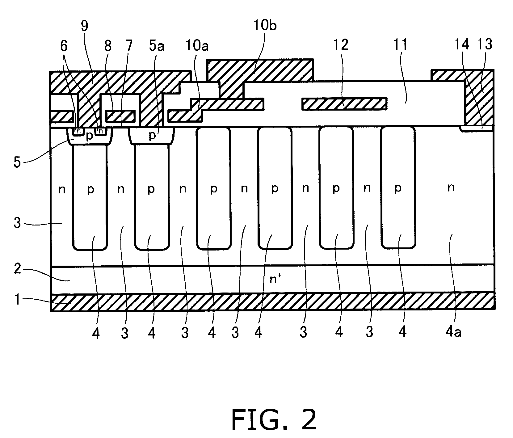
[0053]FIG. 7 is a cross-sectional view schematically showing the configuration of a semiconductor apparatus according to a third embodiment of the invention. More specifically, FIG. 7A is a cross-sectional view corresponding to the structure shown in FIG. 3. In FIG. 7B, the horizontal axis corresponds to the lateral position in the cross-sectional structure of FIG. 7A, and the vertical axis represents impurity concentration in the semiconductor layer on the drain layer 2.

[0054]In this embodiment, the impurity concentration in the super-junction structure (n-type pillar layers 3 and p-type pillar layers 4) of the termination region is lower than the impurity concentration in the super-junction (n-type pillar layers 3 and p-type pillar layers 4) of the device region. By decreasing the impurity concentration in the super-junction structure of the termination region below that of the device region, n-type pillar layers 3 and p-type pillar layers 4 in the termination region are depleted ...


PUM


Abstract

A semiconductor apparatus includes: a first first-conductivity-type semiconductor layer; a second first-conductivity-type semiconductor layer provided on a major surface of the first first-conductivity-type semiconductor layer in a device region and a termination region outside the device region; a third second-conductivity-type semiconductor layer being adjacent to the second first-conductivity-type semiconductor layer, forming a periodic array structure; a field insulating film provided on the second first-conductivity-type semiconductor layer and the third second-conductivity-type semiconductor layer in the termination region; a first field plate electrode provided on the field insulating film and connected to the second main electrode or the control electrode; and a second field plate electrode. The second field plate electrode partly overlies the first field plate electrode through intermediary of an insulating film and extends on the field insulating film outside the first field plate electrode. The second field plate electrode is floating in potential.

Description

CROSS-REFERENCE TO RELATED APPLICATIONS[0001]This application is based upon and claims the benefit of priority from the prior Japanese Patent Application No. 2007-021337, filed on Jan. 31, 2007; the entire contents of which are incorporated herein by reference.BACKGROUND OF THE INVENTION[0002]1. Field of the Invention[0003]This invention relates to a semiconductor apparatus, and more particularly to a vertical semiconductor apparatus suitable for power electronics applications.[0004]2. Background Art[0005]The ON resistance of a vertical power MOSFET (metal-oxide-semiconductor field effect transistor) greatly depends on the electric resistance of its conduction layer (drift layer). The dopant concentration that determines the electric resistance of the drift layer cannot exceed a maximum limit, which depends on the breakdown voltage of a pn junction between the base and the drift layer. Thus there is a tradeoff between the device breakdown voltage and the ON resistance. Improving thi...

Claims


Application Information

Patent Timeline
Patent Type & Authority Applications(United States)
IPC IPC(8): H01L29/78
CPCH01L29/0634H01L29/0878H01L29/7811H01L29/404H01L29/1095
Inventor SAITO, WATARUONO, SYOTARO
Owner KK TOSHIBA
Why Eureka
Try Eureka