Package structure with embedded capacitor, fabricating process thereof and applications of the same

a technology of embedded capacitors and packaging structures, which is applied in the field of packaging structures and fabricating processes thereof, can solve the problems of limited substrate layout space occupied by the embedded capacitors, reduced increased substrate thickness, so as to improve the working performance of the package structure, short circuit layout in the package structure, and save circuit layout space

Inactive Publication Date: 2008-07-31
ADVANCED SEMICON ENG INC
View PDF15 Cites 29 Cited by
  • Summary
  • Abstract
  • Description
  • Claims
  • Application Information

AI Technical Summary

Benefits of technology

[0018]According to one embodiment of the present invention, the techniques of the present invention are characterized in that the two grooves respectively disposed at the opposite sides of the dielectric layer are filled with the conductive material for forming two conductive embedded plates embedded in the dielectric layer correspondingly, and the package structure with the embedded capacitor can be formed by the two conductive embedded plates which have opposite potentials, and by the dielectric layer disposed between the two conductive embedded plates. By adopting the package structure with the embe

Problems solved by technology

However, because a capacitor property (a capacitor value) of the capacitor device is proportional to a dielectric constant of the dielectric material of the device, the dielectric material of the conventional embedded capacitor device cannot go through a high temperature sintering process as the non-embedded ceramic capacitor (usually a strontium titanate group material formed by performing the high temperature sintering process) does; therefore, the dielectric constant of the conventional embedded capacitor is usually smal

Method used


Image

  • Package structure with embedded capacitor, fabricating process thereof and applications of the same
  • Package structure with embedded capacitor, fabricating process thereof and applications of the same
  • Package structure with embedded capacitor, fabricating process thereof and applications of the same

Examples


Embodiment Construction

[0026]The embodiments of the present invention are directed to a package structure with an embedded capacitor. In order to make the aforementioned and other objects, features and advantages of the present invention more comprehensible, embodiments of several package structures with embedded capacitors are described in detail below.

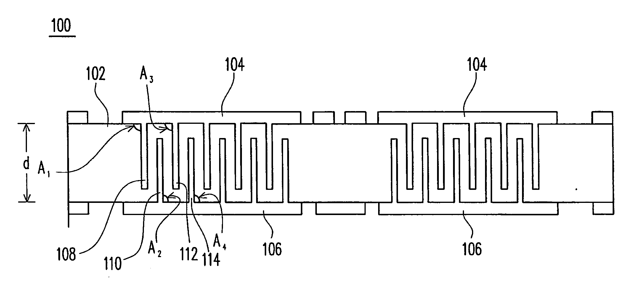
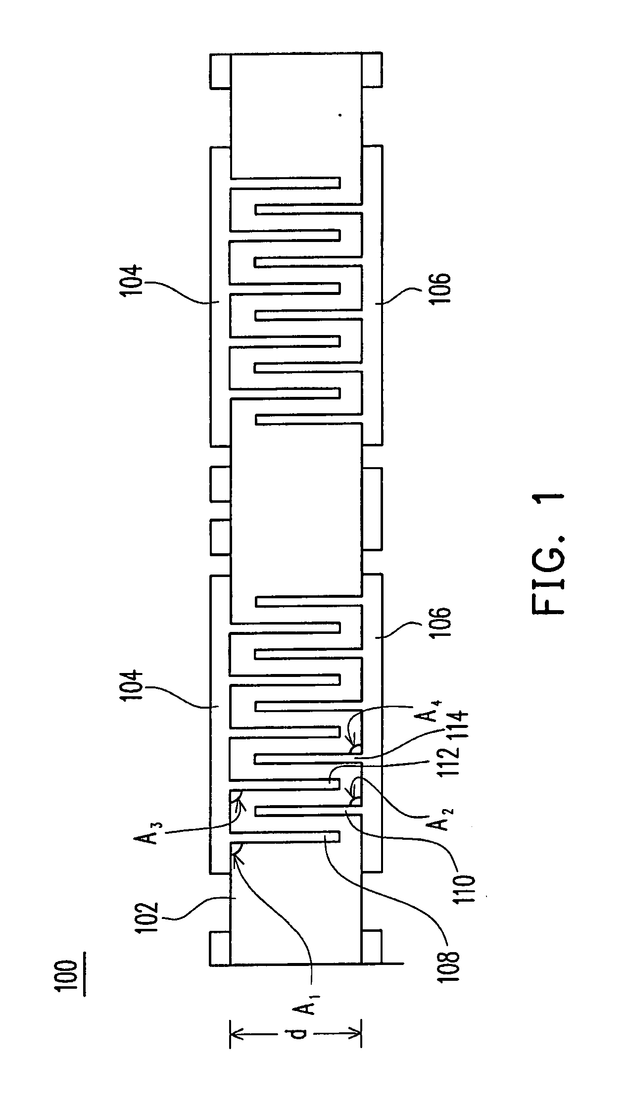
[0027]Please refer to FIG. 1 which illustrates a package structure 100 with an embedded capacitor according to one embodiment of the present invention. The package structure 100 with the embedded capacitor includes: a dielectric layer 102, a first conductive layer 104, a second conductive layer 106, a first embedded plate 108, and a second embedded plate 110. The dielectric layer 102 has a thickness d. In one embodiment of the present invention, the dielectric layer 102 can be a resin substrate in a Resin Clad Copper (RCC) layer. However, in a different embodiment, the dielectric layer 102 is a core dielectric layer in an interlayer circuit board.

[0028]The...


PUM


Abstract

A package structure with an embedded capacitor, a fabricating process thereof and applications of the same are provided, wherein the package structure includes a dielectric layer, a first conductive layer, a second conductive layer, a first embedded plate and a second embedded plate. The dielectric layer has a thickness. The first conductive layer with a first potential is located on one side of the dielectric layer. The second conductive layer with a second potential is located on the dielectric layer at the other side thereof opposite to the first conductive layer. The first embedded plate and the second embedded plate that are embedded in the dielectric layer are separated at a distance, wherein the first embedded plate is electrically connected with the first conductive layer, and the second embedded plate is electrically connected with the second conductive layer.

Description

CROSS-REFERENCE TO RELATED APPLICATION[0001]This application claims the priority benefit of Taiwan application serial no. 96103594, filed on Jan. 31, 2007. The entirety of the above-mentioned patent application is hereby incorporated by reference herein and made a part of this specification.BACKGROUND OF THE INVENTION[0002]1. Field of the Invention[0003]The present invention relates to a package structure and a fabricating process thereof, and in particular, to a package structure with an embedded capacitor, a fabricating process thereof and applications of the same.[0004]2. Description of Related Art[0005]A package structure with an embedded capacitor is a package structure which embeds the capacitor in a substrate with a dielectric material by using a Multiple Stacked Package (MSP) technology, thereby replacing a conventional non-embedded ceramic capacitor for shortening a circuit layout and reducing a required number of non-embedded passive devices, so as to reduce a distance of ...

Claims


Application Information

Patent Timeline
IPC IPC(8): H01L21/283H01G4/228
CPCH01G4/228H01L23/49822H01L23/49833H01L23/50H01L2224/48091H01L2224/48227H01L24/48H05K1/162H05K3/4611H05K2201/09981H01L2924/19041H01L2924/00014H01L2224/45099H01L2224/45015H01L2924/207
Inventor WANG, YUNG-HUIOU, YING-TEHUNG, CHIH-PIN
Owner ADVANCED SEMICON ENG INC
Why Eureka
Try Eureka