Phosphorus Containing Si Epitaxial Layers in N-Type Source/Drain Junctions

a technology of source/drain junction and phosphorus, which is applied in the direction of semiconductor devices, layered products, transportation and packaging, etc., can solve the problems of inability to selectively process, high temperature during a fabrication process, and inability to stabilize csub under excessive thermal stress

Active Publication Date: 2008-07-31
APPLIED MATERIALS INC
View PDF34 Cites 377 Cited by
  • Summary
  • Abstract
  • Description
  • Claims
  • Application Information

AI Technical Summary

Benefits of technology

[0013]In accordance with one embodiment of the present invention the pressure in the process chamber is maintained at about 10 Torr. In one or more embodiments, the n-dopant is phosphorus, and the n-type dopant source comprises phosphine.
[0014]In accordance with one or more embodiments, the silicon source is a higher order silane. According to one or more embodiments of the present invention, the silicon source is selected from the group consisting of trisilane and pentasilane. In certain embodiments, the level of the n-dopant is at least about 8×10²⁰ atoms/cm3. In specific embodiments, the level of the n-dopant is about 1.2×10²¹ atoms/cm3.
[0015]According to one or more embodiments, the temperature during deposition is in a range of about 540° C. and below about 560° C. In accordance with another embodiment, the n-dopant is a capping layer on top of a silicon carbon layer. In one or more embodiments, the epitaxial layer has a tensile stress created by n-dopants in the layer that is equivalent to the tensile stress that can be created by a concentration of substitutional carbon in the epitaxial layer of about 0.55%. In specific embodiments, a measured resistivity in the epitaxial layer is greater than about 0.25 mOhm·cm. and lower than 0.5 mOhm·cm.
[0016]In accordance with a further aspect of the present i

Problems solved by technology

However, Csub is not stable under excessive amounts of thermal stress as the Si:C film is grown under metastable conditions.
Such high temperatures are not desirable during a fabrication process due to thermal budget considerations and possible uncontrolled nitridation reactions to the substrate surface.
), howeve

Method used


Image

  • Phosphorus Containing Si Epitaxial Layers in N-Type Source/Drain Junctions
  • Phosphorus Containing Si Epitaxial Layers in N-Type Source/Drain Junctions
  • Phosphorus Containing Si Epitaxial Layers in N-Type Source/Drain Junctions

Examples


Embodiment Construction

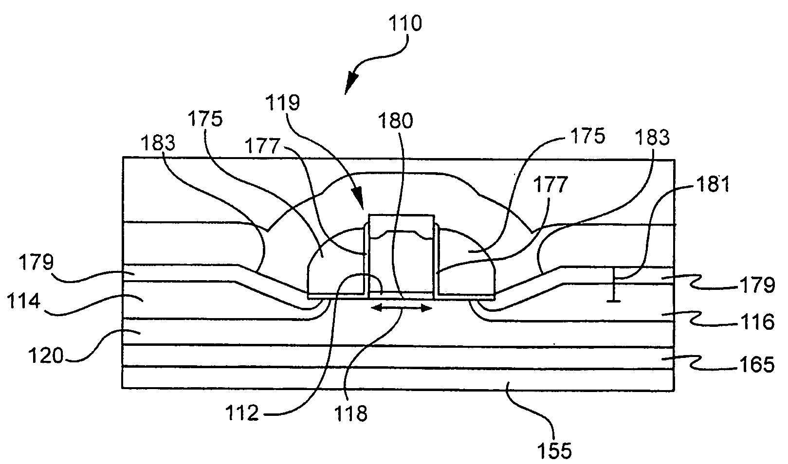
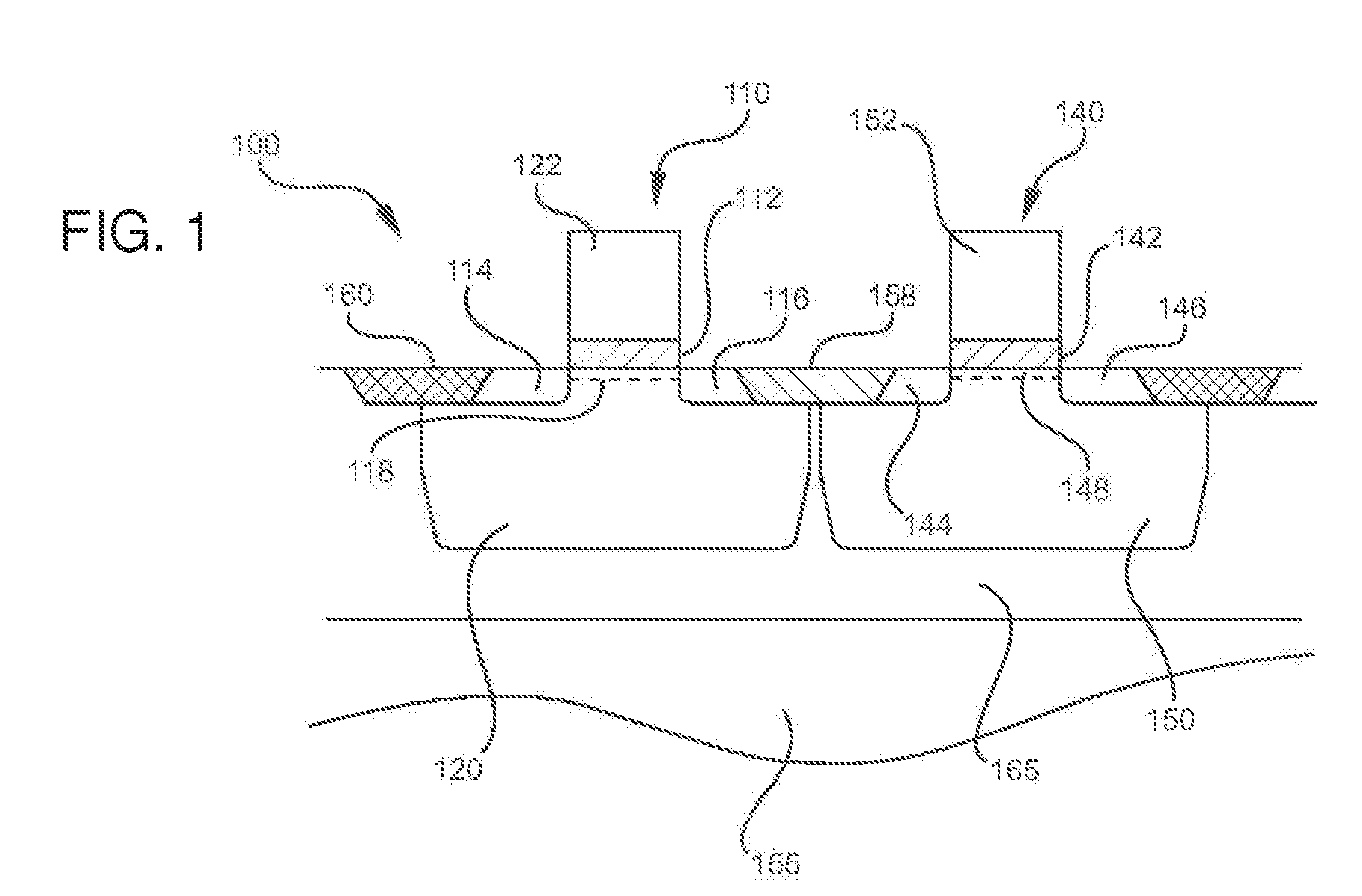
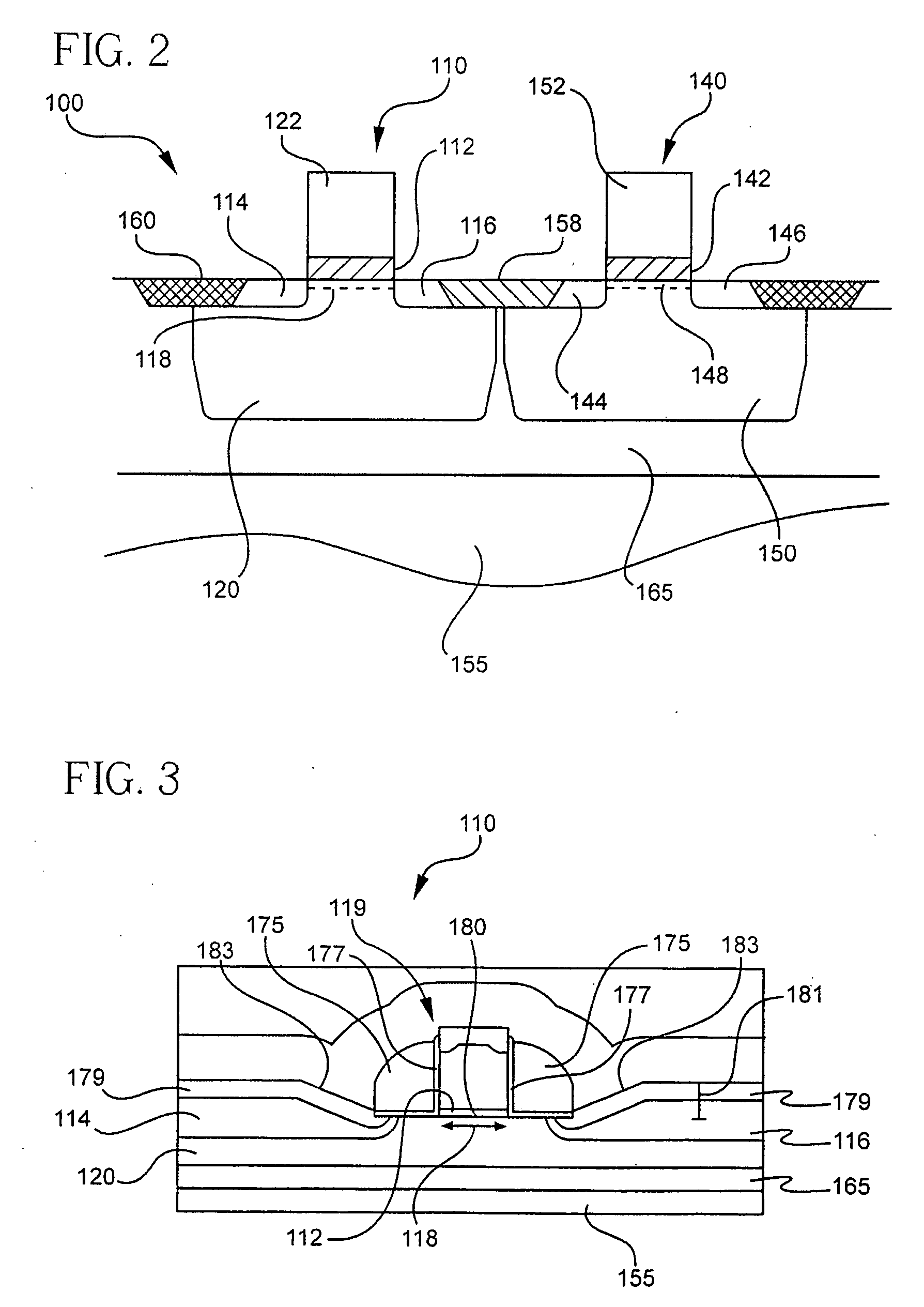
[0027]Embodiments of the invention generally provide methods and apparatus for forming and treating a silicon-containing epitaxial layer. Specific embodiments pertain to methods and apparatus for forming and treating an epitaxial layer during the manufacture of a transistor.

[0028]As used herein, epitaxial deposition refers to the deposition of a single crystal layer on a substrate, so that the crystal structure of the deposited layer matches the crystal structure of the substrate. Thus, an epitaxial layer or film is a single crystal layer or film having a crystal structure that matches the crystal structure of the substrate. Epitaxial layers are distinguished from bulk substrates and polysilicon layers.

[0029]Throughout the application, the terms “silicon-containing” materials, compounds, films or layers should be construed to include a composition containing at least silicon and may contain germanium, carbon, boron, arsenic, phosphorus gallium and / or aluminum. Compounds or alloys of...


PUM

PropertyMeasurementUnit
Temperatureaaaaaaaaaa

Abstract

Methods for formation of epitaxial layers containing n-doped silicon are disclosed. Specific embodiments pertain to the formation and treatment of epitaxial layers in semiconductor devices, for example, Metal Oxide Semiconductor Field Effect Transistor (MOSFET) devices. In specific embodiments, the formation of the n-doped epitaxial layer involves exposing a substrate in a process chamber to deposition gases including a silicon source, a carbon source and an n-dopant source. An epitaxial layer may have considerable tensile stress which may be created in a significant amount by a high concentration of n-dopant. A layer having n-dopant may also have substitutional carbon. Phosphorus as an n-dopant with a high concentration is provided. A substrate having an epitaxial layer with a high level of n-dopant is also disclosed.

Description

RELATED APPLICATION[0001]This application is a continuation-in-part of U.S. application Ser. No. 11 / 609,826 filed Dec. 11, 2006, which is incorporated herein by reference in its entirety.BACKGROUND[0002]Embodiments of the present invention generally relate to methods and apparatus for selective formation of epitaxial layers containing silicon, carbon and a doping material. Specific embodiments pertain to methods and apparatus for the selective formation of n-doped epitaxial layers in semiconductor devices, for example, Metal Oxide Semiconductor Field Effect Transistor (MOSFET) devices.[0003]The amount of current that flows through the channel of a MOS transistor is directly proportional to a mobility of carriers in the channel, and the use of high mobility MOS transistors enables more current to flow and consequently faster circuit performance. Mobility of the carriers in the channel of an MOS transistor can be increased by producing a mechanical stress in the channel. A channel und...

Claims


Application Information

Patent Timeline
IPC IPC(8): H01L21/8236H01L21/20C04B41/50B32B3/00
CPCH01L21/823807H01L21/823814H01L21/823878Y10T428/24612H01L29/66628H01L29/7834H01L29/7848H01L29/1608
Inventor CHOPRA, SAURABHYE, ZHIYUANKIM, YIHWAN
Owner APPLIED MATERIALS INC
Why Eureka
Try Eureka