Manufacturing method of electronic element

Active Publication Date: 2008-08-07
SUMITOMO ELECTRIC IND LTD
View PDF3 Cites 3 Cited by
  • Summary
  • Abstract
  • Description
  • Claims
  • Application Information

AI Technical Summary

Benefits of technology

[0022]An object of the present invention is to provide a technique for preventing breakage of a compound semiconductor epitaxial wafer during processing steps.
[0024]When the wafer thickness t=300 μm, q=about 0.3 mm to 1.5 mm, when the wafer thickness t=350 μm, q=about 0.35 mm to 1.75 mm, and when the wafer thickness t=500 μm, q=about 0.5 mm to 2.5 mm. Although the optimum width q changes according to the wafer thickness, the width may be about 1 mm in many cases. With respect to the etching depth, the circumferential portion is removed until an InP substrate is exposed or to a depth in the range of 0 μm to 10 μm from the surface of the InP substrate (0 μm<s≦10 μm wherein s is the removal amount of the circumferential portion of the substrate). By removing an epitaxial layer in the circumferential portion, cracking of the wafer in the processing steps can be significantly decreased.
[0031]Therefore, the inventors have found that it is effective to remove the epitaxially grown anomalous portion 42 in the circumferential portion. In fact, the removal of the epitaxial layer in the circumferential portion of an epitaxial wafer caused the excellent effect that the wafer was little cracked in the wafer process.
[0032]Since the anomalously elevated portion in the circumferential portion is removed, stress or thermal stress is not produced from the circumferential portion even when a thermal or physical factor such as heating or impact is applied to the wafer. As a result, the wafer is not broken. The present invention is not limited to the manufacture of a light-receiving element on an InP substrate. The present invention can also be used for preventing cracking of a wafer in the process when a light-emitting element such as a laser diode or a light-emitting diode is manufactured on an InP substrate or a GaAs substrate. Further, when not only the epitaxial layer is removed but also the circumferential portion of the substrate is removed to a depth of 0 μm to 10 μm, wafer cracking can be further avoided. In an anomalously epitaxially grown portion, cracking may be caused due to damage to the surface layer of the substrate. In view of removal of a damaged layer, it is meaningless to remove to a depth of more than 10 μm, and the process yield is rather decreased. (In wet etching, etching proceeds in a transverse direction due to side etching, and thus side etching is increased by excessively deep etching, resulting in excessive removal. In dry etching such as RIE, a resist is etched by RIE, and thus a thick resist mask is required for deep etching but has technical difficulty.)
[0033]As in Patent Document 1 (FIG. 5), when the annular groove is formed, an anomalously grown elevated portion remains in the circumferential portion 37 of the epitaxial layer. An impact due to the anomalously grown elevated portion and nonuniform heating cause cracking, and the annular groove additionally increases nonuniformity in strength, thereby further accelerating the occurrence of cracking. The object of the present invention is completely different from that of Patent Document 1, and the technique and results are also different from Patent Document 1.

Problems solved by technology

When the width q of the circumferential removal is larger than 5t, the ratio of wastes in the wafer is excessively increased.
When q is smaller than t, cracking cannot be prevented.

Method used


Image

  • Manufacturing method of electronic element
  • Manufacturing method of electronic element
  • Manufacturing method of electronic element

Examples


first embodiment

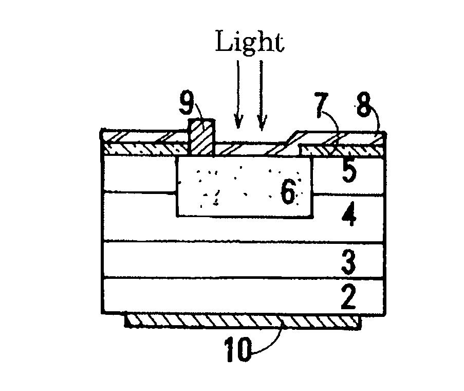
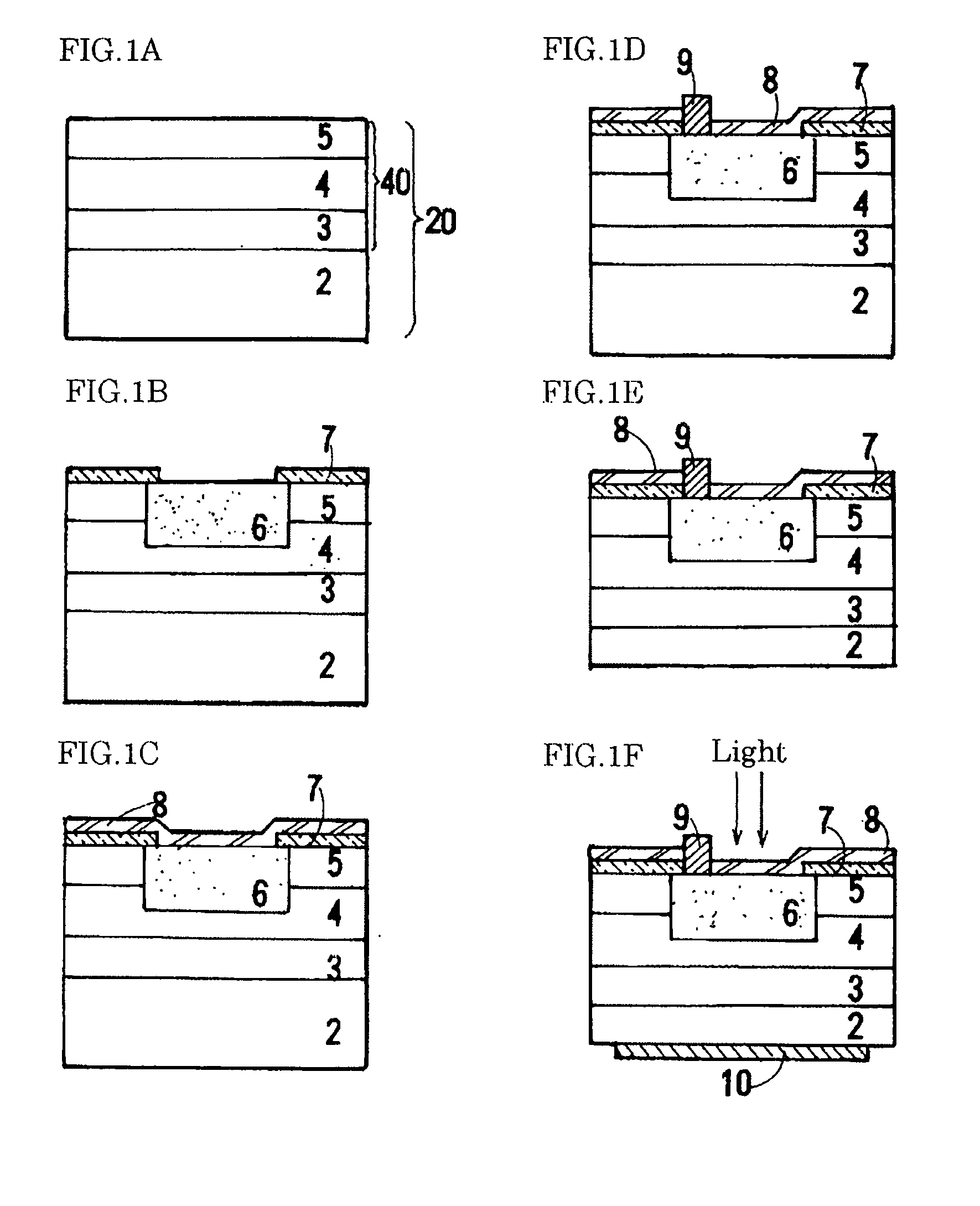
[0050]The gist of the present invention is to remove a circumferential portion of an epitaxial wafer including compound semiconductor thin films epitaxially grown on an InP or GaAs substrate. As a result, an anomalously grown portion which is an elevated portion in the circumferential portion can be completely removed, and thus the wafer is little broken in subsequent processing steps (wafer process).

[0051]In order to selectively remove only the circumferential portions of the epitaxial layers, the entire surface of the epitaxial wafer is masked and covered with a resist, and a mask is formed by development so as to cover a central portion excluding only the circumferential portion of the resist. Then, the epitaxial layers are removed using a liquid etchant or RIE. The epitaxial layers are composed of InP and InGaAs, and thus when the etchant is used, it is necessary to change the etchant because suitable etchants for the respective epitaxial layers are different. Namely, HCl is use...


PUM


Abstract

A circumferential portion of an epitaxial wafer is removed to remove an anomalously grown elevated portion formed in a circumferential chamfer. An epitaxial layer in the circumferential portion is removed with a width q=t to 5t wherein t is the thickness of the epitaxial layer so that the surface of a substrate is exposed. Therefore, cracking of the epitaxial layer in processing steps can be prevented.

Description

BACKGROUND OF THE INVENTION[0001]1. Field of the Invention[0002]The present invention relates to a technique for preventing cracking of a wafer in a wafer process for manufacturing semiconductor devices such as light-emitting elements and light-receiving elements.[0003]2. Description of the Background Art[0004]Processing of devices using InP and GaAs may cause cracking of an epitaxial wafer during the process. When a 2-inch or 3-inch wafer is processed, cracking of the wafer during the process makes it impossible to further continue the process and thus makes the wafer defective.[0005]Although the process may be continued using a cracked wafer, transport and lithography become difficult because of the indeterminate form of pieces of the broken wafer. Therefore, it is necessary to find conditions suitable for the form and to manually process the pieces. Even when a device is manufactured on a piece of the broken wafer by various techniques in a time-consuming manner, much labor is re...

Claims


Application Information

Patent Timeline
IPC IPC(8): H01L21/302
CPCH01L31/184Y02E10/544H01L33/0062Y02P70/50
Inventor IGUCHI, YASUHIROMITSUI, NOBUYUKI
Owner SUMITOMO ELECTRIC IND LTD
Why Eureka
Try Eureka