Self-aligned epitaxial growth of semiconductor nanowires

a technology of semiconductor nanowires and epitaxial growth, which is applied in the direction of nanoinformatics, crystal growth process, polycrystalline material growth, etc., can solve the problem of difficulty in precisely placing the wires at the desired location

Inactive Publication Date: 2008-08-14
GLOBALFOUNDRIES INC
View PDF19 Cites 44 Cited by
  • Summary
  • Abstract
  • Description
  • Claims
  • Application Information

AI Technical Summary

Benefits of technology

[0007]In another embodiment, a method of forming a nanostructure comprises: forming a mask on a surface of a substrate, wherein the mask has at least one opening to expose a portion of the surface of the masked substrate; cleaning the exposed surface of the masked substrate with dilute aqueous hydrofluoric acid solution; plating metal particles of a metal for catalyzing semiconductor nanowire growth on the exposed surface of the masked substrate to form a plated substrate by immersing the masked substrate and an anode into a plating solution containing a metal particle precursor for the metal particles, and applying an electrical plating current for a predetermined time across the masked substrate and anode, wherein the metal particle precursor is gold, indium, or alloys thereof, the plating current is −1 mA/cm2 to −100 mA/cm2, the plating time is less than or equal to 10 seconds, and light illumination is optionally applied to the masked substrate, wherein the size and the density of the metal particles are tuned by changing plating conditions comprising plating current, plating potential, plating time, agitation, temperature, illumination of the substrate, concentration of the metal species in the plating solution, addition of other chemical species to the plating solution, concentration of other chemical species in the plating solution, or a combination comprising at least one of these plating conditions; cleaning the plated substrate with dilute aqueous hydrofluoric acid solution; annealing the plated substrate prior to growing nanowires, wherein annealing is carried out at 300 to 550° C. for 10 minutes to 2 hours in an inert or reducing atmosphere, cleaning the plated substrate after annealing, with dilute aqueous hydrofluoric acid solution, and growing nanowires on the plated substrate

Problems solved by technology

However, a key challenge for the integration of such nanowires into real device is the difficulty in placing the wires precisely at desired locations.
However, the present methods for growth of such nanowires provide non-site specific me

Method used


Image

  • Self-aligned epitaxial growth of semiconductor nanowires
  • Self-aligned epitaxial growth of semiconductor nanowires
  • Self-aligned epitaxial growth of semiconductor nanowires

Examples


Embodiment Construction

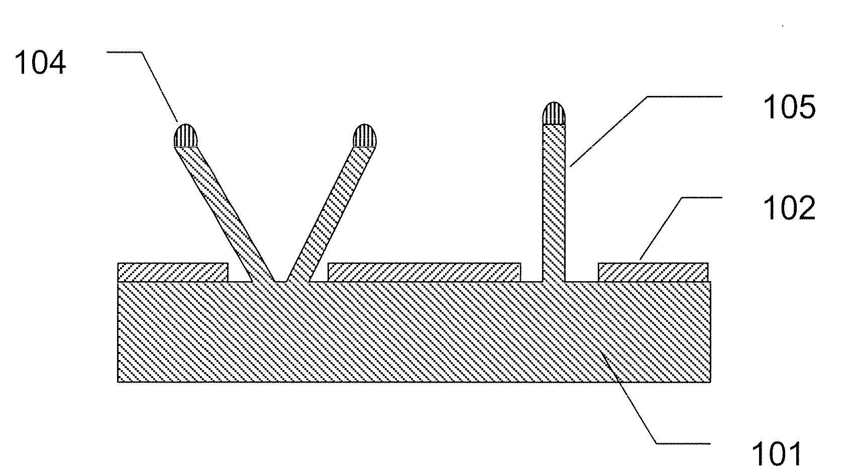
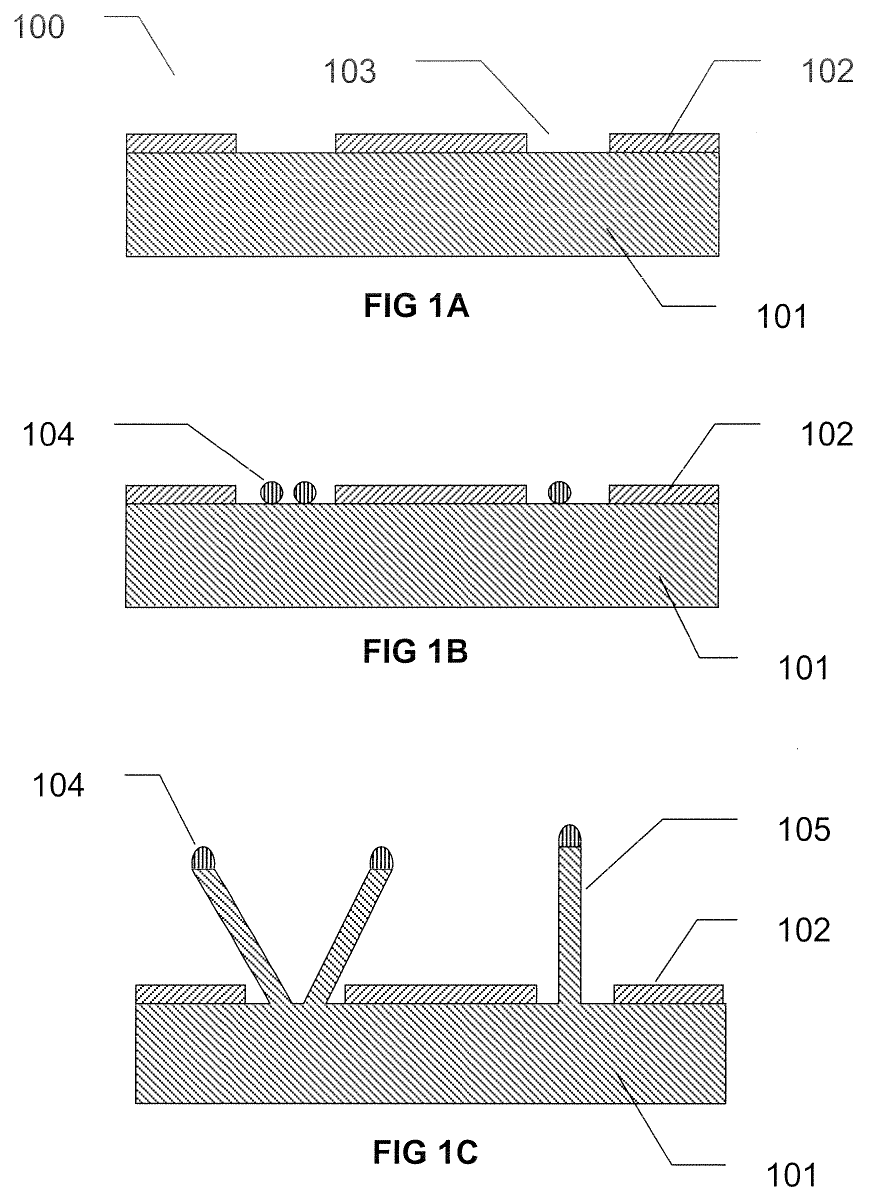
[0013]A method of producing self-aligned epitaxial semiconductor nanowires on substrates is disclosed. The method includes plating (i.e., depositing) metal particles on a patterned substrate having cleaned, exposed regions; annealing the plated metal particles on the substrate; and growing nanowires from the plated metal particles by a VLS process at a predetermined temperature in an apparatus having a chamber, with a nanowire precursor gas (e.g., silane SiH4 for silicon nanowires; germane GeH4 for germanium nanowires; and the like). The diameter of the nanowire prepared by this method is proportional to the size (i.e., diameter) of the metal particle, specifically to the diameter of the hemispherical metal particle as measured at the interface of the metal particle and the substrate. The method selectively provides metal particles for catalyzing growth of nanowires on the surface of the substrate to thereby provide patterns of metal particles on the surface of the substrate, using ...


PUM


Abstract

Disclosed herein is a method of forming a nanostructure having nanowires by forming a mask with at least one opening on a surface of a substrate, to expose a portion of the surface of the substrate; depositing particles of a metal capable of catalyzing semiconductor nanowire growth on the exposed surface of the substrate by electroplating or electroless plating; and growing nanowires on the plated substrate with a precursor gas by a vapor-liquid-solid (VLS) process. Also disclosed is a nanostructure including nanowires prepared by the above method.

Description

FIELD OF THE INVENTION[0001]The present invention relates to a method for forming self-aligned semiconductor nanowires. More particularly, this invention relates to a method of electrochemically or electrolessly depositing metal nanoparticles at specific locations on a substrate to catalyze formation of epitaxial semiconductor nanowires at these locations by vapor-liquid-solid growth process.BACKGROUND OF THE INVENTION[0002]Inorganic nanowires, sometimes referred to as “whiskers”, can be grown on surfaces by a vapor-liquid-solid (VLS) process as described in U.S. Pat. Nos. 3,493,431, 5,702,822, and 5,858,862. As disclosed therein, semiconductor nanowires grown by VLS process, such as Si, Ge, GaAs and InP nanowires, are of particular interest for fabricating integrated electronic devices based on nanowire field effect transistors (FETs). Nanowire FETs can exhibit the advantageous quantum effects and also allow for 3-dimensional device integration, and hence may provide a much higher ...

Claims


Application Information

Patent Timeline
IPC IPC(8): H01L29/06H01L21/20
CPCB82Y10/00H01L2221/1094C30B29/60H01L21/0237H01L21/02381H01L21/02521H01L21/02603H01L21/02639H01L21/02642H01L21/02645H01L21/02653H01L21/28525H01L29/0665H01L29/0673H01L29/0676C30B11/12
Inventor COHEN, GUY MOSHEDELIGIANNI, HARIKLIAHUANG, QIANGROMANKIW, LUBOMYR T.
Owner GLOBALFOUNDRIES INC
Why Eureka
Try Eureka