
Bumping process and bump structure

a technology of bumping process and bump structure, which is applied in the direction of semiconductor devices, electrical equipment, semiconductor/solid-state device details, etc., can solve the problems of limiting the size and performance of chips, increasing the cost of bumping process, so as to reduce the pad density and reduce the pad density. , the effect of reducing the pad density

Inactive Publication Date: 2008-08-14
ELAN MICROELECTRONICS CORPORATION
View PDF3 Cites 16 Cited by
  • Summary
  • Abstract
  • Description
  • Claims
  • Application Information

AI Technical Summary

Benefits of technology

The present invention provides a structure and process for a planarized bump to overcome the drawbacks of conventional art. A passivation layer with a planarized surface is formed to cover a pad on a substrate, and the layer is etched to form a hole penetrating therethrough to expose a contact surface of the pad. A bump is then formed on the contact surface and the planarized surface. The structure includes several layers with different hardness in stack, and the contact surface has a shape of stripe. The planarized surface provides a larger effective region, allowing for a smaller pad and increased mechanical strength at the peripheral of the pad. The bump has a larger effective area, reducing the likelihood of short circuit and current leakage, improving the yield of the pressing process and the conductive quality for the pad.

Problems solved by technology

In order to reduce electrical noises and to increase adhesion and conductivity, gold is typically used for the bump material, which makes the bumping process expensive and difficult.
Therefore, improving the bump structure and bumping process becomes an important issue.
On the other hand, the density and performance of a package limit the size and performance of a chip.
As the size of IC shrinks, the IC package becomes the bottleneck to further shrink the IC, if the density and performance of the package are not enhanced, for example the size and pitch of the bumps are limited or the conductivity of the bumps are not good enough.
However, the contact density of the chip is thus lowered and the chip size cannot be minimized.
There's difficulty to solve this problem using conventional techniques.
Even though the semiconductor process is capable to minimize the chip size, the backend package does not catch up with the IC shrinkage and thus limits the minimized size of the chip.
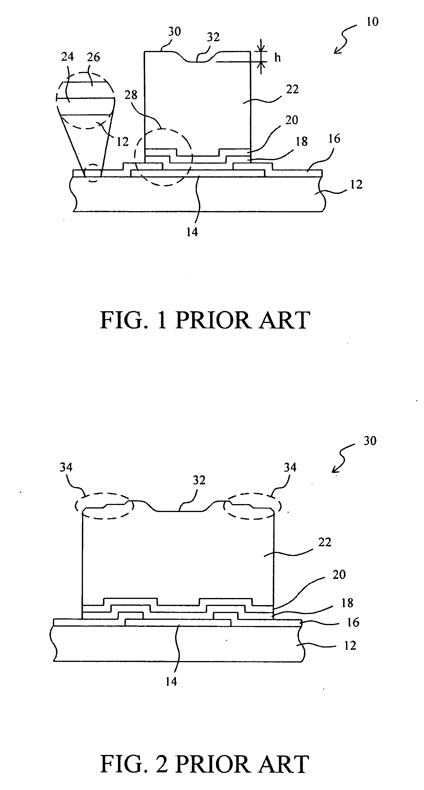
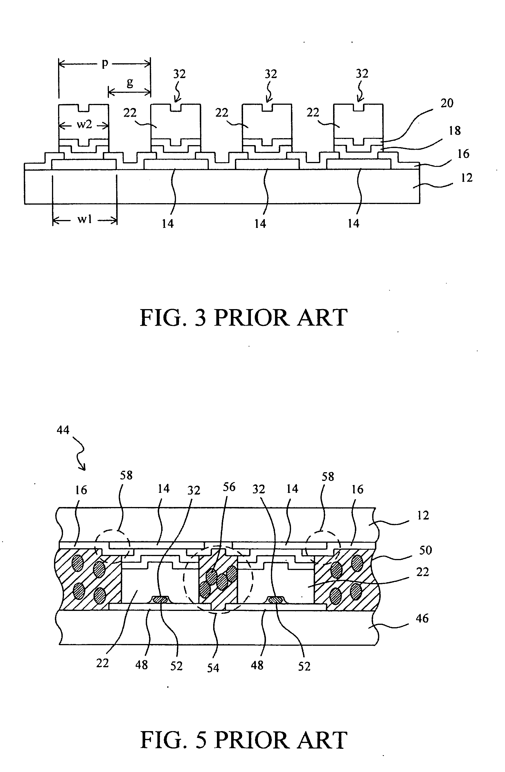
Further, a conventional bump structure has drawbacks during the pressing process.
However, if the conductive particles 52 are larger, then there will be fewer of them to be trapped in the effective region 32, and thus there's greater contact impedance and poor conduction quality after the pressing process.
Therefore, there's unbeatable difficulty in conventional technology.
Furthermore, an elemental drawback of flip chip package is the weak mechanical strength at the peripheral region 58 of the bump 22, and damage happens easily due to lateral force.

Method used


Image

  • Bumping process and bump structure
  • Bumping process and bump structure
  • Bumping process and bump structure

Examples


Embodiment Construction

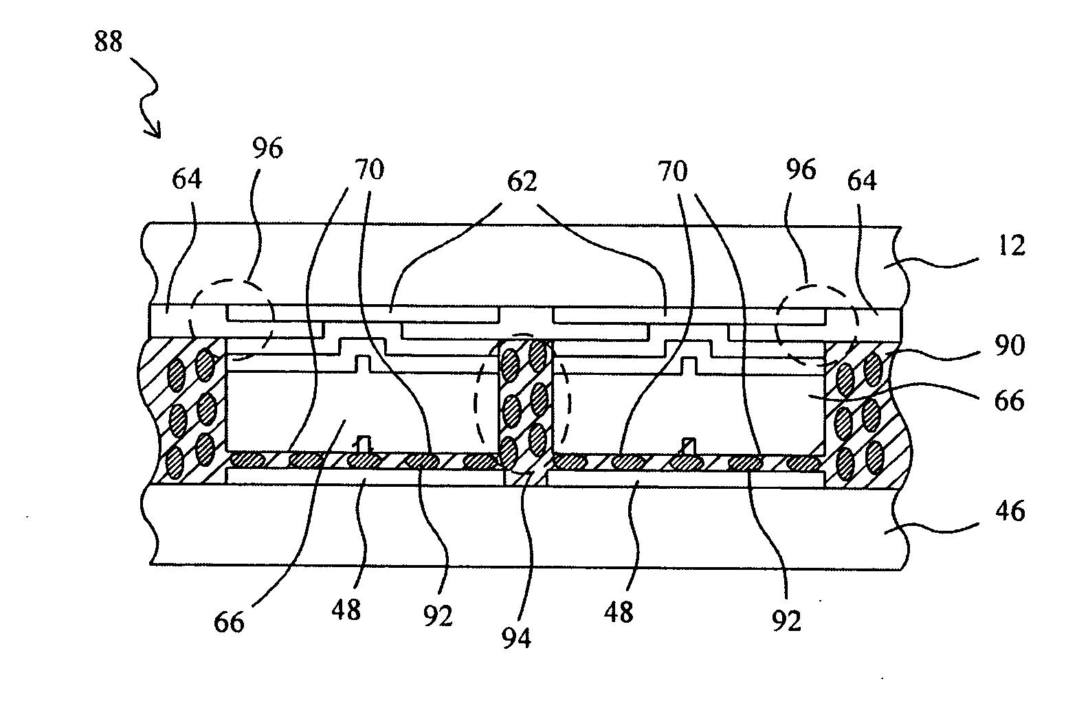
[0026]FIGS. 6A and 6B show a gold bump structure 60 according to the present invention, and FIGS. 7A and 7B show the top views, in which FIG. 6A is a cross-sectional view along the X direction and FIG. 6B is a cross-sectional view along the Y direction. Referring to FIGS. 6A and 6B, in the gold bump structure 60, a passivation layer 64 has a planarized surface and covers a portion of each pad 62 on a substrate 12, a UBM 18 and a gold film 20 are stacked on the pad 62 and passivation layer 64, and a gold bump 66 is on the gold film 20. The pad 62 is made of aluminum, aluminum alloy, or other metal or highly conductive alloy, and the passivation layer 64 comprises one or more layers of silicon dioxide, silicon oxide, silicon nitride, silicon oxy nitride, or other superior chemical resistive materials or their combination to protect the circuits within the substrate 12. The UBM 18 is used mainly to protect the pad 62 from being penetrated by any chemical particles during the following ...


PUM


Abstract

A bumping process comprises forming a passivation layer having a planarized surface covering a pad on a substrate, forming a hole penetrating through the passivation layer to expose a contact surface of the pad, and forming a bump on the contact surface and planarized surface. The planarized surface will provide a larger effective area for pressing, thereby minimizing the pad, enhancing the mechanical strength at the peripheral of the pad, providing more selection flexibility for anisotropic conductive film, reducing the possibilities of short circuit and current leakage within the bump gap, and increasing the yield of the pressing process and the conductive quality of the bump.

Description

RELATED APPLICATIONS[0001]This application is a Divisional patent application of co-pending application Ser. No. 11 / 404,750, filed on 17 Apr. 2006. The entire disclosure of the prior application Ser. No. 11 / 404,750, from which an oath or declaration is supplied, is considered a part of the disclosure of the accompanying Divisional / Continuation application and is hereby incorporated by reference.FIELD OF THE INVENTION[0002]The present invention is generally related to a bumping process and bump structure, and more particularly, to a planarized bump structure and a bumping process therefor.BACKGROUND OF THE INVENTION[0003]Wire bonding, tape automated bonding (TAB) and flip chip bonding are popular packages for integrated circuits (ICs). Generally, wire bonding is used in low-density package with less than 300 inputs / outputs (I / Os). In high-density packages, up to 600 I / Os may be provided by TAB, and flip chip package provides much higher package density with more than 600 I / Os. In fli...

Claims


Application Information

Patent Timeline
Patent Type & Authority Applications(United States)
IPC IPC(8): H01L23/485
CPCH01L24/03H01L24/05H01L2224/293H01L2224/81903H01L2924/01076H01L2924/01033H01L2924/01006H01L24/11H01L24/83H01L2224/0401H01L2224/05624H01L2224/13099H01L2224/13144H01L2224/83851H01L2924/01004H01L2924/01013H01L2924/01014H01L2924/01015H01L2924/01022H01L2924/01027H01L2924/01074H01L2924/01078H01L2924/01079H01L2924/05042H01L2924/14H01L2924/3011H01L24/13H01L2224/13016H01L2924/00014
Inventor HU, CHUN-PINGCHEN, CHENG-CHUNGTSI, CHIEN-WENLEE, YU-CHING
Owner ELAN MICROELECTRONICS CORPORATION
Learn More