Semiconductor, semiconductor device, complementary transistor circuit device

a technology of complementary transistors and semiconductors, applied in the direction of semiconductor devices, thermoelectric device junction materials, electrical apparatus, etc., can solve the problems of difficult circuit design or the like, difficult to achieve practical use of circuits, and difficult to control the conductivity type of channels by doping with impurities, so as to facilitate the formation of organic semiconductor layers, reduce the production cost of the entire circuit device, and reduce the effect of production cos

Inactive Publication Date: 2008-08-21
IDEMITSU KOSAN CO LTD
View PDF13 Cites 54 Cited by
  • Summary
  • Abstract
  • Description
  • Claims
  • Application Information

AI Technical Summary

Benefits of technology

[0027]A semiconductor with such a configuration is ambipolar and operates stably. Operation becomes more stable if the oxide semiconductor layer is formed of an n-type oxide semiconductor. The application of a semiconductor can be diversified due to the stable operation.
[0037]The above configuration enables the semiconductor to have improved characteristics.
[0045]The semiconductor device exhibits ambipolar characteristics due to the use of the above-mentioned semiconductor as a semiconductor. Further, due to the combination of the organic semiconductor layer and the oxide semiconductor layer, the semiconductor in this semiconductor device can operate stably.
[0050]Due to the use of the above-mentioned ambipolar semiconductor device, the circuit device is free from the need of separated provision of an n-type semiconductor device and a p-type semiconductor device, which leads to a reduced production cost of the entire circuit device.
[0051]The semiconductor of the invention contributes a reduction in production cost since formation of the organic semiconductor layer can be facilitated. Further, due to the combination of the organic semiconductor layer and the oxide semiconductor layer, the semiconductor of the invention exhibits ambipolar characteristics and operates stably. Therefore, the semiconductor of the invention can be used more widely.
[0053]In the complementary transistor circuit device of the invention, separate fabrication of an n-type semiconductor device and a p-type semiconductor device is unnecessary due to the use of the above-mentioned semiconductor device, leading to a reduction in production cost of the entire circuit device.

Problems solved by technology

Using such an organic semiconductor in a TFT encounters a problem that control of the conductivity type of a channel by doping with impurities is difficult as compared with the case where amorphous or polycrystalline silicon is used in a TFT.
However, since the n-channel type TFT and the p-channel type TFT are fabricated separately using different organic substances, such a circuit is difficult to be put into a practical use due to a complicated production process and an increased production cost.
Therefore, only a limited material selection is permitted, which may make circuit design or the like difficult.
Normal pentacene exhibits only p-type characteristics, which may make production of a semiconductor device difficult and costly.
However, the technologies disclosed in Patent Documents 4 and 5 have such disadvantages that operation of the semiconductor and the semiconductor device using thereof tends to be unstable due to the combined use of an organic substance having n-type characteristics and an organic substance having p-type characteristics.

Method used


Image

  • Semiconductor, semiconductor device, complementary transistor circuit device
  • Semiconductor, semiconductor device, complementary transistor circuit device
  • Semiconductor, semiconductor device, complementary transistor circuit device

Examples


first embodiment

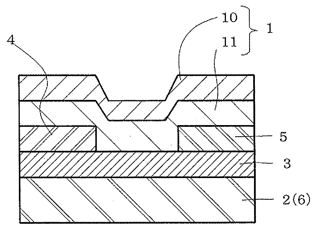
[0075]FIG. 1 shows a schematic cross-sectional view of the semiconductor and the semiconductor device according to the first embodiment of the invention.

[0076]As shown in FIG. 1, the semiconductor device of this embodiment is provided with a semiconductor 1, a first electrode 2, an insulating layer 3 interposed between the semiconductor 1 and the first electrode 2, a second electrode 4 disposed nearer to the semiconductor 1 than the insulating layer 3, and a third electrode 5 which is detached from the second electrode 4 and disposed nearer to the semiconductor 1 than the insulating layer 3. The semiconductor 1 of this embodiment is formed of an organic semiconductor layer 10 and an oxide semiconductor layer 11.

[0077]This semiconductor device, which can be used as a field effect transistor (FET), a light-emitting element, a light-receiving element, and the like, has a configuration that the layers in the form of a thin film are stacked on a substrate 6.

[0078]Specifically, the semico...

second embodiment

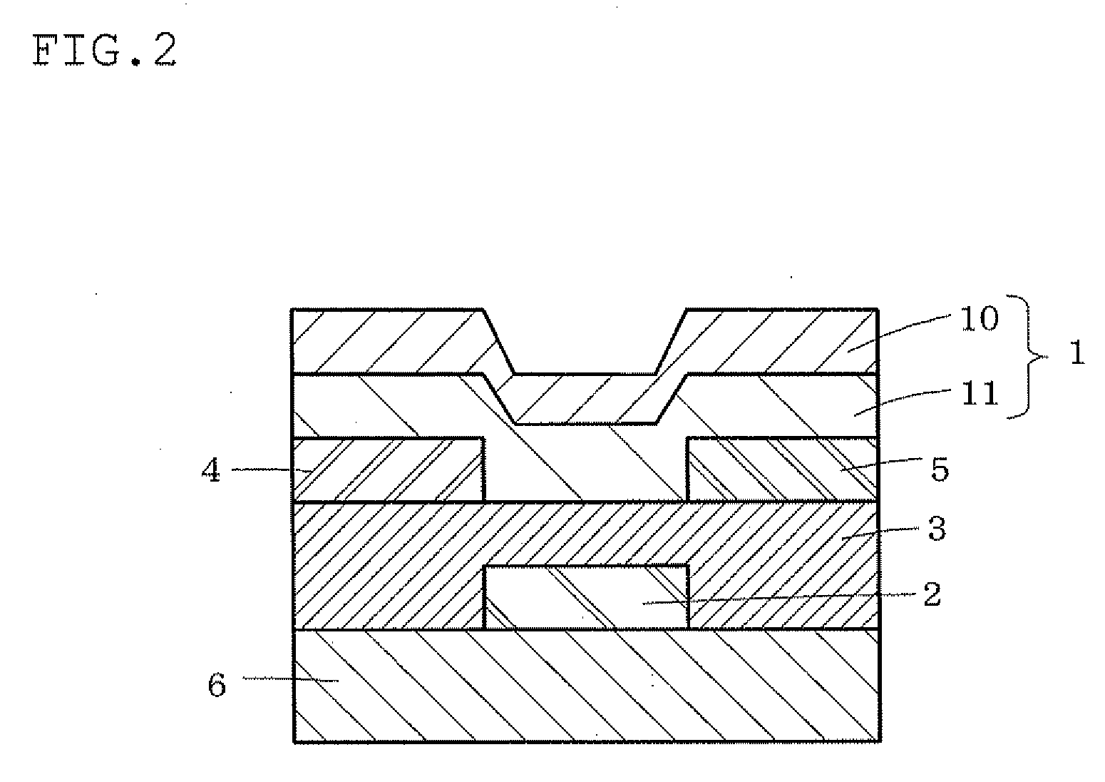
[0163]FIG. 2 shows a schematic cross sectional view of the semiconductor and the semiconductor device according to the second embodiment of the invention.

[0164]The semiconductor device of this embodiment is substantially similar to the semiconductor device in the first embodiment, except that the substrate 6 and the first electrode 2 are provided separately.

[0165]Specifically, in the semiconductor and the semiconductor device in this embodiment, the first electrode 2 is separately provided in the middle of the substrate 6. This first electrode 2 is formed of the material used in the second and third electrodes 4 and 5 in the first embodiment. The insulating layer 3 is provided on the substrate 6 as well as on the first electrode 2.

[0166]Except for the above, the configuration of the semiconductor and the semiconductor device in this embodiment is the same as that in the first embodiment.

[0167]The semiconductor device in this embodiment is used as a field effect transistor as in the ...

third embodiment

[0169]FIG. 3 shows a schematic cross sectional view of the semiconductor and the semiconductor device according to the third embodiment of the invention.

[0170]In the semiconductor device of this embodiment, unlike the semiconductors of the above-mentioned embodiments, the second and third electrodes 4 and 5 are not interposed between the insulating layer 3 and the oxide semiconductor layer 11, and are provided on the top of the organic semiconductor layer 10.

[0171]Since the insulating layer 3, the oxide semiconductor layer 11, and the organic semiconductor layer 10 are all provided between the first electrode 2(6) and the second and third electrodes 4 and 5, a field can be applied effectively to allow the semiconductor characteristics to be developed easily. In addition, the second and third electrodes 4 and 5 are in direct contact with the organic semiconductor layer 10, the semiconductor easily develops ambipolar characteristics even when mobility of the organic semiconductor is l...


PUM


Abstract

A semiconductor device including a semiconductor 1, a first electrode 2, an insulating layer 3 interposed between the semiconductor 1 and the first electrode 2, the second electrode 4 which is in contact with the semiconductor 1 and is detached from the first electrode 2, and the third electrode 5 which is in contact with the semiconductor 1 and is detached from the first electrode 2 and the second electrode 4, wherein the semiconductor 1 is provided with the organic semiconductor layer 10 and the oxide semiconductor layer 11.

Description

TECHNICAL FIELD[0001]The invention relates to a semiconductor provided with ambipolar characteristics which is used in a thin film transistor (hereinafter abbreviated as “TFT”) or the like, a semiconductor device using the semiconductor, and a complementary transistor circuit device using the semiconductor device.BACKGROUND[0002]In recent years, an organic semiconductor using an organic substance has attracted attention as a semiconductor for a TFT.[0003]Generally, organic substances used in an organic semiconductor have such advantages that not only they can be formed into a thin film by a relatively easy film-forming method such as spin coating and vacuum vapor deposition, but also they can produce a TFT at low temperatures as compared with a conventional TFT which is prepared using amorphous or polycrystalline silicon. Processing at low temperatures enables formation of a film on a plastic substrate having a low heat resistance. As a result, various effects such as a decreased di...

Claims


Application Information

Patent Timeline
Patent Type & Authority Applications(United States)
IPC IPC(8): H01L51/00
CPCH01L51/0525H01L51/0587H01L51/0562H01L51/0545H10K10/472H10K10/486H10K10/466H10K10/29
Inventor YANO, KOKINAKANOTANI, HAJIMEADACHI, CHIHAYA
Owner IDEMITSU KOSAN CO LTD
Why Eureka
Try Eureka