Structure for metal cap applications

a technology of metal caps and structures, applied in the direction of semiconductor devices, semiconductor/solid-state device details, electrical apparatus, etc., can solve the problems of delay in using metallic capping layers, affecting the reliability of prior art interconnect structures, etc., to improve the reliability, improve the strength of dielectric breakdown, and improve the effect of technology extendibility

Inactive Publication Date: 2008-08-21
GLOBALFOUNDRIES INC
View PDF10 Cites 44 Cited by
  • Summary
  • Abstract
  • Description
  • Claims
  • Application Information

AI Technical Summary

Benefits of technology

[0009]The present invention provides an interconnect structure (of the single or dual damascene type) and a method of forming the same, which removes unwanted metallic residue from the surface of the dielectric material which is located between each metallic capped conductive feature. The inventive interconnect structure has improved dielectric breakdown strength as compared to prior art interconnect structures. The inventive interconnect structure has better reliability and technology extendibility for the semiconductor industry.

Problems solved by technology

The presence of the metallic residue 22 between each of the conductive features hinders the reliability of the prior art interconnect structure 10 and has delayed using metallic capping layers for the last three generations.

Method used


Image

  • Structure for metal cap applications
  • Structure for metal cap applications
  • Structure for metal cap applications

Examples


first embodiment

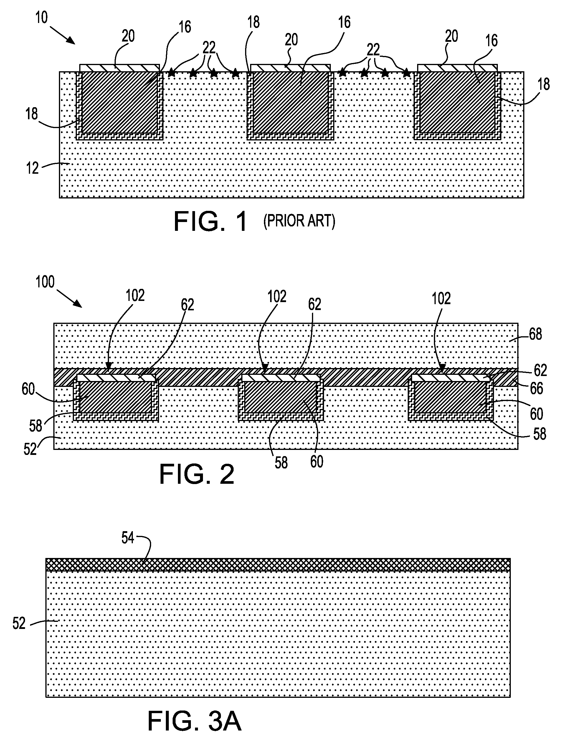
[0028]FIG. 3A shows an initial structure that is employed in the present invention. As illustrated, the initial structure includes a dielectric material 52 which contains a sacrificial dielectric layer 54 on an upper surface of the dielectric material 52. The dielectric material 52 is typically located on a surface of a substrate (not shown).

[0029]The substrate, which is not shown, may comprise a semiconducting material, an insulating material, a conductive material or any combination thereof. When the substrate is comprised of a semiconducting material, any semiconductor such as Si, SiGe, SiGeC, SiC, Ge alloys, GaAs, InAs, InP and other III / V or II / VI compound semiconductors may be used. In addition to these listed types of semiconducting materials, the present invention also contemplates cases in which the semiconductor substrate is a layered semiconductor such as, for example, Si / SiGe, Si / SiC, silicon-on-insulators (SOIs) or silicon germanium-on-insulators (SGOIs).

[0030]When the ...

second embodiment

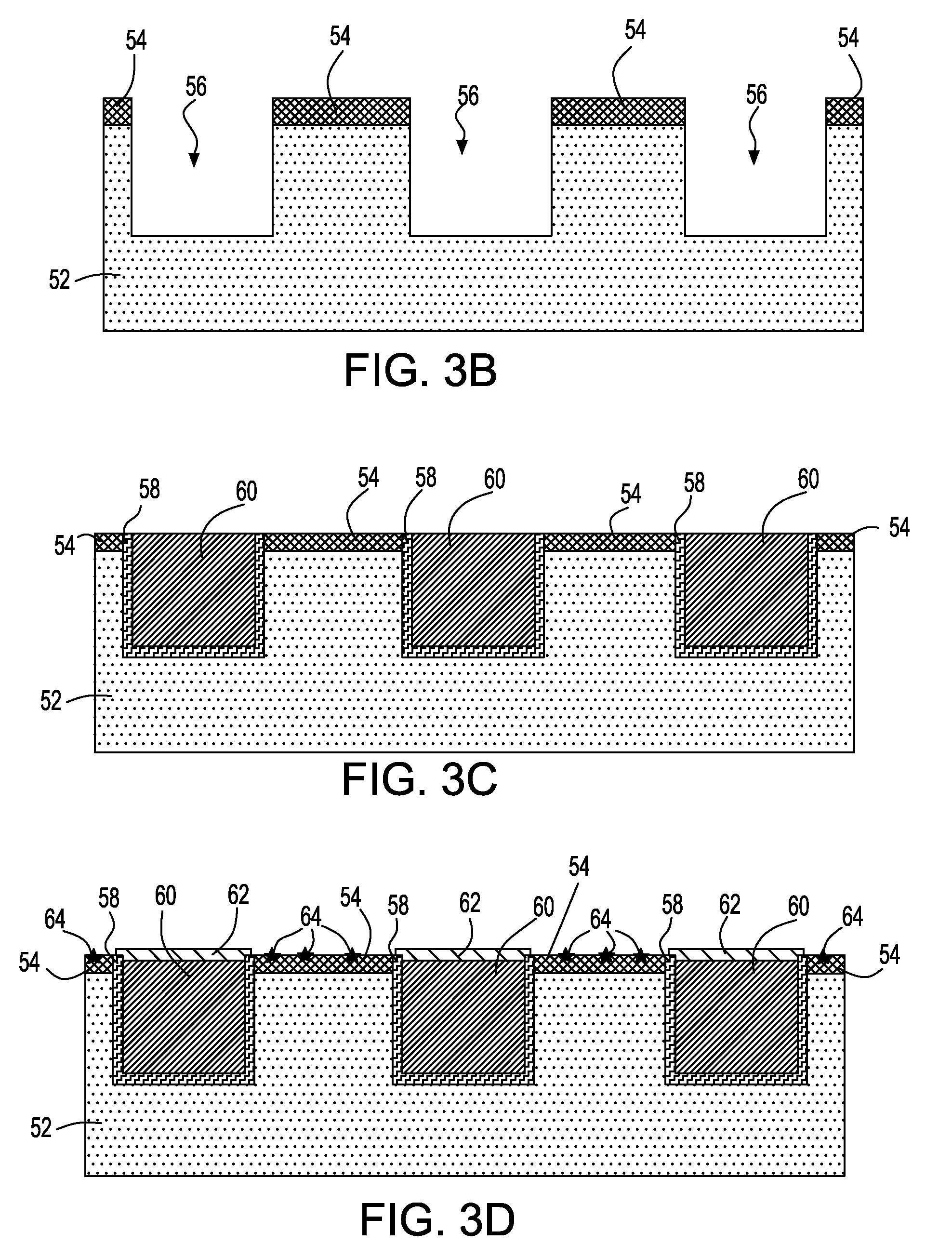
[0052]FIG. 4B shows the structure after forming at least one opening 56 into the structure shown in FIG. 4A. The at least one opening 56 is formed as described above and the various types of openings mentioned above are also contemplated herein for the present invention.

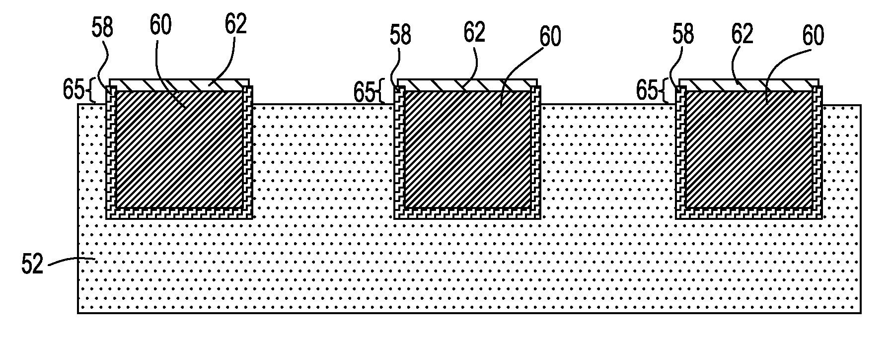
[0053]FIG. 4C shows the structure after filling the at least one opening 56 with a diffusion barrier 58 and a conductive material 60 and after planarization. During the planarization process, the polishing selective layer 70 is removed. The second embodiment then proceeds by utilizing the processing steps associated with FIGS. 3D-3F above. After forming the dielectric capping layer 66 that encapsulates the extended top portion of the metallic capped conductive feature, the other dielectric material 68 is optionally formed as described above.

third embodiment

[0054]FIGS. 5A-5D illustrates the present invention which differs from that of the first two embodiments described above. In this embodiment, a chemical, e.g., oxygen, nitrogen, ammonia and / or hydrogen plasma process is used to remove the metallic residue from the structure.

[0055]The third embodiment of the present invention begins by providing the structure shown in FIG. 3B utilizing the processing steps described above. Following the formation of the structure shown in FIG. 3B, and subsequent filling of the at least one opening 56 with a diffusion barrier 58 and a conductive material 60, a planarization process such as, for example, chemical mechanical polishing and / or grinding, is employed to provide the structure shown in FIG. 5A. As shown, the planarization process completely removes the sacrificial dielectric layer 54 from the structure such that the upper surfaces of the diffusion barrier 58, the conductive material 60, and the dielectric material 62 are substantially coplana...


PUM

PropertyMeasurementUnit
dielectric constantaaaaaaaaaa
thicknessaaaaaaaaaa

Abstract

An interconnect structure is provided in which the conductive features embedded within a dielectric material are capped with a metallic capping layer, yet no metallic residue is present on the surface of the dielectric material in the final structure. The inventive interconnect structure has improved dielectric breakdown strength as compared to prior art interconnect structures. Moreover, the inventive interconnect structure has better reliability and technology extendibility for the semiconductor industry. The inventive interconnect structure includes a dielectric material having at least one metallic capped conductive feature embedded therein, wherein a top portion of said at least one metallic capped conductive feature extends above an upper surface of the dielectric material. A dielectric capping layer is located on the dielectric material and it encapsulates the top portion of said at least one metallic capped conductive feature that extends above the upper surface of dielectric material.

Description

FIELD OF THE INVENTION[0001]The present invention relates to a semiconductor structure and a method of fabricating the same. More particularly, the present invention relates to an interconnect structure that has better reliability and technology extendibility for the semiconductor industry.BACKGROUND OF THE INVENTION[0002]Generally, semiconductor devices include a plurality of circuits which form an integrated circuit (IC) fabricated on a semiconductor substrate. A complex network of signal paths will normally be routed to connect the circuit elements distributed on the surface of the substrate. Efficient routing of these signals across the device requires formation of multilevel or multilayered schemes, such as, for example, single or dual damascene wiring structures. The wiring structure typically includes copper, Cu, since Cu based interconnects provide higher speed signal transmission between large numbers of transistors on a complex semiconductor chip as compared with aluminum,...

Claims


Application Information

Patent Timeline
Patent Type & Authority Applications(United States)
IPC IPC(8): H01L23/48H01L21/4763
CPCH01L21/76826H01L21/76834H01L21/76885H01L21/76849H01L21/7684
Inventor YANG, CHIH-CHAOEDELSTEIN, DANIEL C.WONG, KEITH KWONG HONYANG, HAINING
Owner GLOBALFOUNDRIES INC
Why Eureka
Try Eureka