Supercharge Your Innovation With Domain-Expert AI Agents!

Circuit with fuse/Anti-fuse transistor with selectively damaged gate insulating layer

Inactive Publication Date: 2008-08-21
SAMSUNG ELECTRONICS CO LTD
View PDF6 Cites 17 Cited by
  • Summary
  • Abstract
  • Description
  • Claims
  • Application Information

AI Technical Summary

Problems solved by technology

The use of laser energy is generally limited to sequential programming processes for fuses and anti-fuses, but such processes take considerable time.
In addition, laser systems are quite expensive and their operation sometimes results in contamination problems.
Thus, it may be difficult to improve the integration density of an integrated circuit device incorporating the control circuit.
In addition, application of the high dielectric breakdown voltage may cause related programming failures.
Furthermore, the reliability of a corresponding driving circuit may deteriorate under the effects of a relatively high voltage required for fuse programming.

Method used


Image

  • Circuit with fuse/Anti-fuse transistor with selectively damaged gate insulating layer
  • Circuit with fuse/Anti-fuse transistor with selectively damaged gate insulating layer
  • Circuit with fuse/Anti-fuse transistor with selectively damaged gate insulating layer

Examples


Embodiment Construction

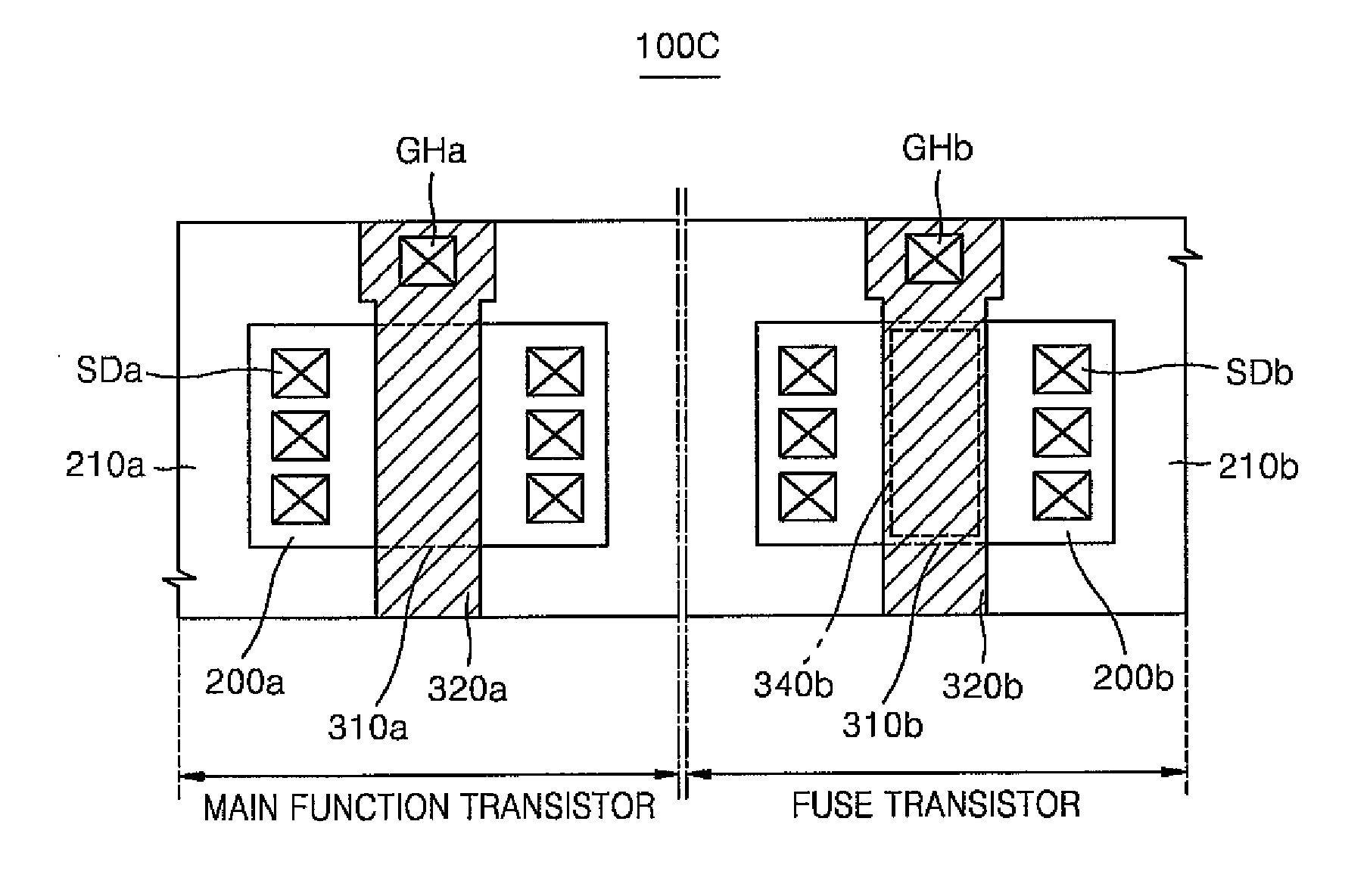
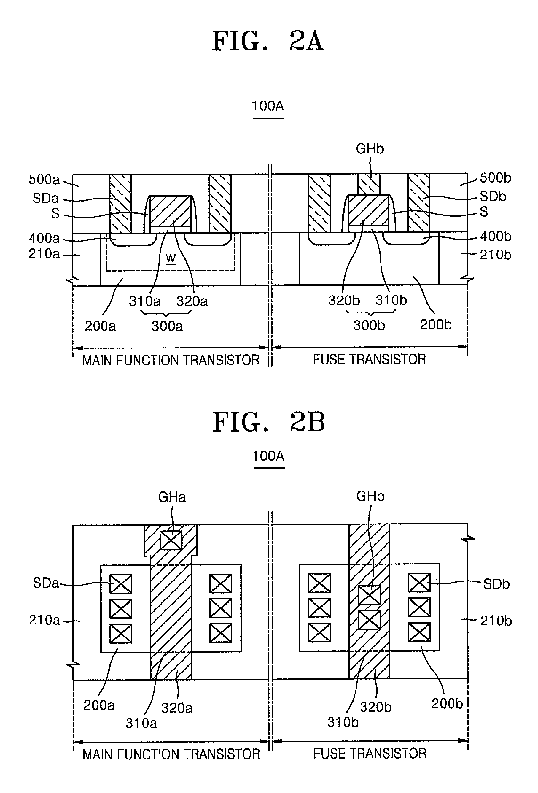
[0018]Several embodiments of the invention will now be described with reference to the accompanying drawings. The invention may, however, be embodied in many different forms and should not be construed as being limited to only the illustrated embodiments.

[0019]Elements and semiconductor regions shown in the drawings are not necessarily drawn to scale, and the dimensions of certain layers and regions may have been exaggerated for clarity. Throughout the drawings and written description, like reference numerals are used to denote like or similar elements.

[0020]In the description, when a layer is referred to as being “on” another layer or substrate, it may be directly on the other layer or substrate, or intervening layers may also be present. Also, although numerical terms (e.g., “first” and “second”) are used herein to describe various members, parts, regions, layers and / or sections, these members, parts, regions, layers and / or sections are not to be limited by these terms. These term...


PUM


Abstract

A semiconductor integrated circuit is disclosed which includes a main transistor and at least one of a fuse transistor or an anti-fuse transistor (“fuse / anti-fuse transistor”). Each transistor type includes an active region formed in a semiconductor substrate, a gate stack comprising a gate insulation layer and a gate electrode sequentially formed on the active region, and source / drain regions separated across the gate stack, but the gate insulation layer of the fuse / anti-fuse transistor is selectively damaged during fabrication.

Description

CROSS-REFERENCE TO RELATED PATENT APPLICATION[0001]A claim of priority is made to Korean Patent Application No. 10-2007-0016796, filed Feb. 16, 2007, in the Korean Intellectual Property Office, the disclosure of which is incorporated herein in its entirety by reference.BACKGROUND OF THE INVENTION[0002]1. Field of the Invention[0003]The present invention relates generally to semiconductor integrated circuits. More particularly, the invention relates to semiconductor integrated circuits including a fuse and / or an anti-fuse.[0004]2. Description of the Related Art[0005]A semiconductor integrated circuit such as a memory device and a logic device may utilize a trimming circuit or a redundancy circuit to remedy the effects of certain circuit defects commonly generated during fabrication. For example, a redundant circuit is sometimes fabricated in parallel with a primary circuit. The primary circuit is then tested, and if it is functioning properly, the redundant circuit may be removed or ...

Claims


Application Information

Patent Timeline
IPC IPC(8): H01H37/76
CPCG11C17/18H01L23/5252H01L23/5256H01L27/11206H01L27/101H01L27/112H01L27/0617H01L2924/0002H10B20/20H10B20/00H01L2924/00H01L21/82
Inventor LIM, JUN-HEESHIN, CHOONG-SUN
Owner SAMSUNG ELECTRONICS CO LTD
Features
  • R&D
  • Intellectual Property
  • Life Sciences
  • Materials
  • Tech Scout
  • Unparalleled Data Quality
  • Higher Quality Content
  • 60% Fewer Hallucinations
Learn More