
Display apparatus, method of driving a display, and electronic device

Inactive Publication Date: 2008-08-21
SONY CORP
View PDF2 Cites 42 Cited by
  • Summary
  • Abstract
  • Description
  • Claims
  • Application Information

AI Technical Summary

Benefits of technology

[0017]By configuring the pixel circuit so as to have the function of eliminating the effects of the variation in the threshold voltage, it is possible to improve the uniformity in brightness over the screen. However, of various parameters of the characteristics of the polysilicon thin film transistor, not only the threshold voltage but also the mobility μ varies from one transistor to another. As can be seen from the transistor characteristic equation described above, the variation in mobility μ can lead to a variation in the drain current Ids even if the gate voltage Vgs is equal. As a result, the intensity of emitted light varies from one pixel to another, and thus degradation occurs in uniformity of brightness over the screen. There is a technique to configure the pixel circuit so as to have a function of eliminating the effects of the variation in mobility in addition to that in threshold voltage of the driving transistor (for example, see Japanese Unexamined Patent Application Publication No. 2006-215213).
[0019]In view of the above, it is desirable to provide a display apparatus capable of accurately correcting light intensity regardless of leakage currents of light emitting elements. Thus, according to an embodiment of the present invention, there is provided a display apparatus including a pixel array and a driving unit adapted to drive the pixel array, the pixel array including scanning lines disposed in the form of rows, signal lines disposed in the form of columns, and pixels disposed, in the form of an array, at respective intersections of the scanning lines and the signal lines, each pixel including at least a sampling transistor, a driving transistor, a light emitting element, and a storage capacitor, a control terminal of the sampling transistor being connected to a corresponding scanning line, one of two current terminals of the sampling transistor being connected to a corresponding signal line and the control terminal of the driving transistor, one of two current terminals of the driving transistor being connected to the light emitting element and the other one being connected to a power supply line, the storage capacitor being connected between the control terminal and one of the two current terminals of the driving transistor, the driving unit being configured to output a control signal over a selected scanning line to turn on the sampling transistor connected to the selected scanning line, and output an image signal over a selected signal line to write the image signal in the storage capacitor via the turned-on sampling transistor, whereby the driving transistor supplies a driving current, depending on a signal voltage of the written image signal, to the light emitting element during a predetermined light emission period, while the driving transistor supplies no driving current during a non-light emission period, each pixel including correction means and a switching transistor, the correction means being adapted to operate in the non-light emission period so as to write a correction voltage in the storage capacitor thereby to eliminate an effect of a variation in a characteristic of the driving transistor, the switching transistor being disposed between one of the two current terminals of the driving transistor and the light emitting element, and the switching transistor being adapted to turn off during the non-light emission period thereby to electrically disconnect the light emitting element from the one of the two current terminals of the driving transistor thereby preventing a leakage current from flowing through the light emitting element during the period in which the correction means operates and thus preventing the correction voltage from having an error due to the leakage current.
[0020]The correction means may additively write a correction voltage corresponding to a threshold voltage of the driving transistor into the storage capacitor so as to eliminate an effect of a variation in the threshold voltage of the driving transistor. The correction means may subtract a correction voltage depending on a mobility of the driving transistor from the signal voltage of the image signal written in the storage capacitor so as to eliminate an effect of a variation in the mobility of the driving transistor.
[0021]The present invention provides great advantages as described below. That is, in the display apparatus according to the embodiment of the present invention, a switching transistor is disposed between the source serving as a current output terminal of a driving transistor and the anode of a light emitting element. During the non-light emission period, the switching transistor is turned off to electrically disconnect the anode of the light emitting element from the source of the driving transistor. In this period, the correction means operates such that a correction voltage is written into the storage capacitor from the current output terminal (source) of the driving transistor so as to eliminate the effects of the variation in characteristic of the driving transistor. Because the anode of the light emitting element is electrically disconnected from the source of the driving transistor during the non-light emission period, no leakage current flows through the light emitting element and thus the potential of the current output terminal of the driving transistor does not have an error due to the leakage current. This makes it possible for the display apparatus to accurately make the correction without being influenced by leakage currents of light emitting elements, and thus it is possible to improve the uniformity in brightness over the screen.
[0022]In the correction process, it is necessary to apply the signal potential from the signal line to the control terminal (gate) of the driving transistor even in the non-light emission period. The cathode of the light emitting element is maintained at a predetermined fixed cathode potential. In the case where the anode of the light emitting element is connected to the source of the driving transistor during the correction process as in the related technique, it is necessary to adjust the relative signal potential with respect to the cathode potential to achieve high accuracy in the correction process. In contrast, in the embodiment of the invention, because the anode of the light emitting element is electrically disconnected from the source of the driving transistor during the correction process, it is allowed to set the signal potential applied to the gate of the driving transistor and the cathode potential of the cathode of the light emitting element independently of each other. Thus, the signal potential and the cathode potential can be properly set so as to achieve low power consumption of the panel and / or low cost.

Problems solved by technology

Although the passive matrix address scheme needs a simpler configuration, the disadvantage of this scheme is that it is difficult to realize a large-size high-resolution display.

Method used


Image

  • Display apparatus, method of driving a display, and electronic device
  • Display apparatus, method of driving a display, and electronic device
  • Display apparatus, method of driving a display, and electronic device

Examples


first embodiment

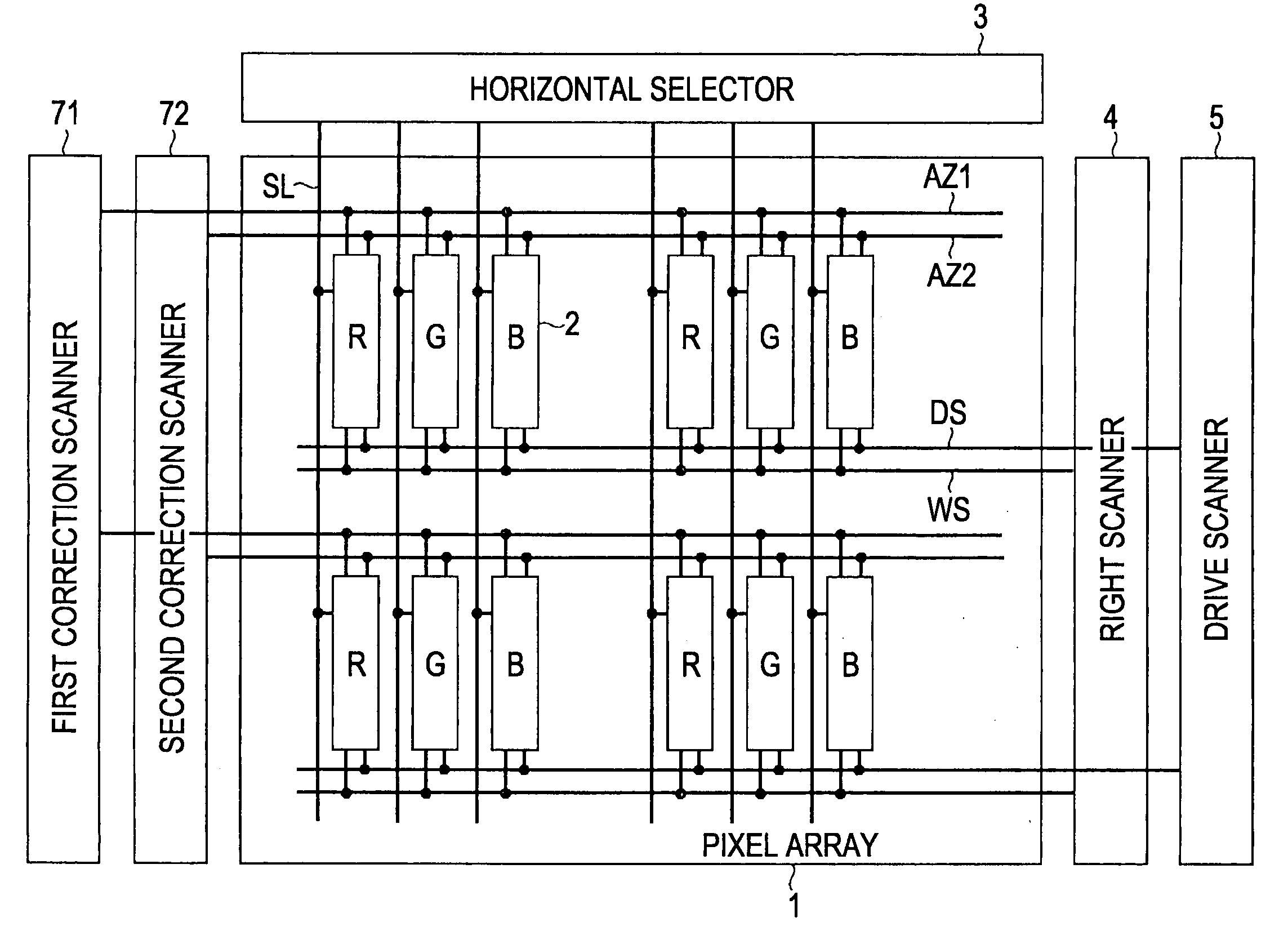
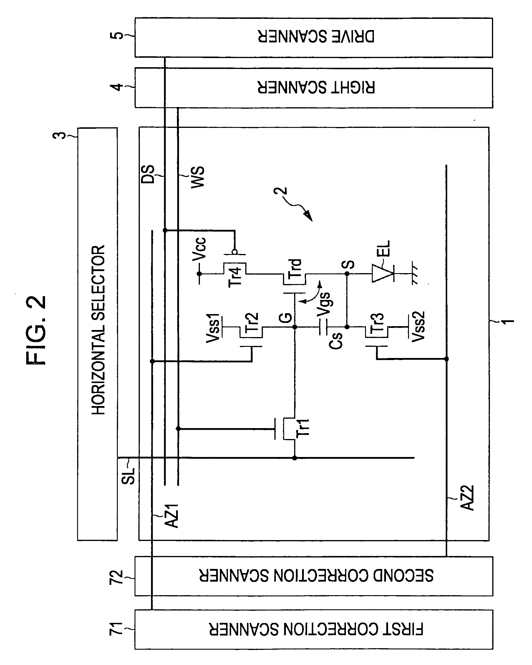
[0068]As shown in FIG. 5, in the present invention, the display apparatus basically includes a pixel array 1 and a driving unit adapted to drive the pixel array 1. The pixel array 1 includes scanning lines WS extending in the row direction, signal lines SL extending in the column direction, and pixels 2 disposed in an array form at respective intersections of the scanning lines WS and the signal lines SL. Each pixel 2 includes, at least, a sampling transistor Tr1, a driving transistor Trd, a light emitting element EL, and a storage capacitor Cs. The control terminal (the gate) of the sampling transistor Tr1 is connected to one of the scanning lines WS. The current terminals (the source and the drain) of the sampling transistor Tr1 are respectively connected to one of the signal lines SL and the control terminal (the gate G) of the driving transistor Trd. One of the current terminals (the source and the drain) of the driving transistor Trd is connected to the light emitting element E...

second embodiment

[0102]FIG. 10 is a timing chart provided for an explanation of the operation of the circuit shown in FIG. 9. In FIG. 6, for ease of understanding, similar reference symbols to those in the timing chart shown in FIG. 8 are used. As shown in FIG. 10, at time T1, the switching transistor Tr4 is turned off to switch the pixel 2 from the light emission state into the non-light emission state. Thereafter, at time T1a, the scanning line DS2 is switched to the low level to turn off the switching transistor Tr6. As a result, the light emitting element EL is electrically disconnected from the driving transistor Trd. Thereafter, in a period from T2 to T3, a preliminary process is performed. Furthermore, in a period from T3 to T4, the threshold voltage correction process is performed. In a period from T5 to T7, the image signal is written in the storage capacitor Cs. In this process, the mobility correction is performed in a period from T6 to T7. In these processes, the light emitting element ...

third embodiment

[0121]FIG. 14 is a timing chart provided for an explanation of the operation of the pixel circuit shown in FIG. 13. This timing chart is basically similar to that shown in FIG. 12 and similar parts to those in FIG. 12 are denoted by similar reference symbols. As shown in FIG. 14, at time T1, the switching transistor Tr4 is turned off, and thus the non-light emission period starts. At time T1a, the switching transistor Tr6 is turned off thereby electrically disconnecting the light emitting element EL from the driving transistor Trd. Note that the turning-off of the switching transistors Tr4 and Tr6 may be performed in the reverse order. Thereafter, the threshold voltage correction process, the image signal sampling process, and the mobility correction process are sequentially performed. Then, at time T7, the sampling transistor Tr1 is turned off to disconnect the gate G of the driving transistor Trd from the signal line SL. Thus, the preliminary process, the correction processes, an...


PUM


Abstract

In a display apparatus including a correction unit and a switching transistor, the correction unit operates in a non-light emission period such that a correction voltage for eliminating an effect of a variation in a characteristic of a driving transistor is stored in a storage capacitor. The switching transistor is disposed between one current terminal of the driving transistor and a light emitting element. The switching transistor turns off during the non-light emission period thereby to electrically disconnect the light emitting element from the one current terminal of the driving transistor thereby preventing a leakage current from flowing through the light emitting element during the period in which the correction unit operates, and thus preventing the correction voltage from having an error due to the leakage current.

Description

CROSS REFERENCES TO RELATED APPLICATIONS[0001]The present invention contains subject matter related to Japanese Patent Application JP 2007-041196 filed in the Japanese Patent Office on Feb. 21, 2007, the entire contents of which are incorporated herein by reference.BACKGROUND OF THE INVENTION[0002]1. Field of the Invention[0003]The present invention relates to a display apparatus including an array of pixels each including a light emitting element, and more particularly, to an active matrix display apparatus adapted to control currents flowing through light emitting elements, for example, of the organic electroluminescent type by using insulating gate field effect transistors disposed in the respective pixels. The present invention also relates to a method of driving such a display apparatus and to an electronic device using such a display apparatus.[0004]2. Description of the Related Art[0005]In an image display apparatus such as a liquid crystal display, a large number of liquid c...

Claims


Application Information

Patent Timeline
IPC IPC(8): G09G3/30
CPCG09G3/3233G09G2300/0819G09G2300/0861H01L27/1255G09G5/10G09G3/3258G09G2320/0233H10K59/871G09G3/30G09G3/32G09G3/20H05B33/12H10K50/824H10K50/841H10K50/8426H10K59/38H10K59/123H10K59/124H10K59/131H10K59/1213H10K59/1216G09G3/3208G09G2310/0289G09G2320/0214
Inventor YAMASHITA, JUNICHITOMIDA, MASATSUGUUCHINO, KATSUHIDE
Owner SONY CORP
Features
  • Generate Ideas
  • Intellectual Property
  • Life Sciences
  • Materials
  • Tech Scout
  • Unparalleled Data Quality
  • Higher Quality Content
  • 60% Fewer Hallucinations
Learn More