Fast axis beam profile shaping by collimation lenslets for high power laser diode based annealing system

a laser diode and beam profile technology, applied in the field of laser thermal processing of semiconductor substrates, can solve the problems of insufficient cure time of pre-ion implantation amorphization defects, short time that the wafer needs to stay at the highest temperature, and long annealing process tim

Active Publication Date: 2008-09-04
APPLIED MATERIALS INC
View PDF26 Cites 41 Cited by
  • Summary
  • Abstract
  • Description
  • Claims
  • Application Information

AI Technical Summary

Problems solved by technology

The time that the wafer needs to stay at the highest temperature can be very short.
One problem recently encountered is that some annealing processes requires a longer time at or near the peak temperature (1300 degrees C.
However, it may be insufficient to completely cure pre-ion implantation amorphization defects.
Amorphization prevents such channeling by ion bombardment of the wafer with heavier atomic species (oxygen, nitrogen, carbon), causing bombardment damage to at least partially convert the active semiconductor layer from a crystalline state to an amorphous state.
Furthermore, conversion of the amorphized region back to a crystalline state essentially forms an epitaxial crystalline layer over the bulk crystalline layer, giving rise to another class of defects, namely boundary defects at the interface between the bulk crystal and the re-crystallized surface.
Unfortunately, if the Gaussian beam profile is widened by a given factor, then the slope of the leading edge of the Gaussian beam profile is reduced by approximately the same factor.
Thus, widening the beam profile along the fast axis does not appear to be possible.

Method used


Image

  • Fast axis beam profile shaping by collimation lenslets for high power laser diode based annealing system
  • Fast axis beam profile shaping by collimation lenslets for high power laser diode based annealing system
  • Fast axis beam profile shaping by collimation lenslets for high power laser diode based annealing system

Examples


Embodiment Construction

Introduction:

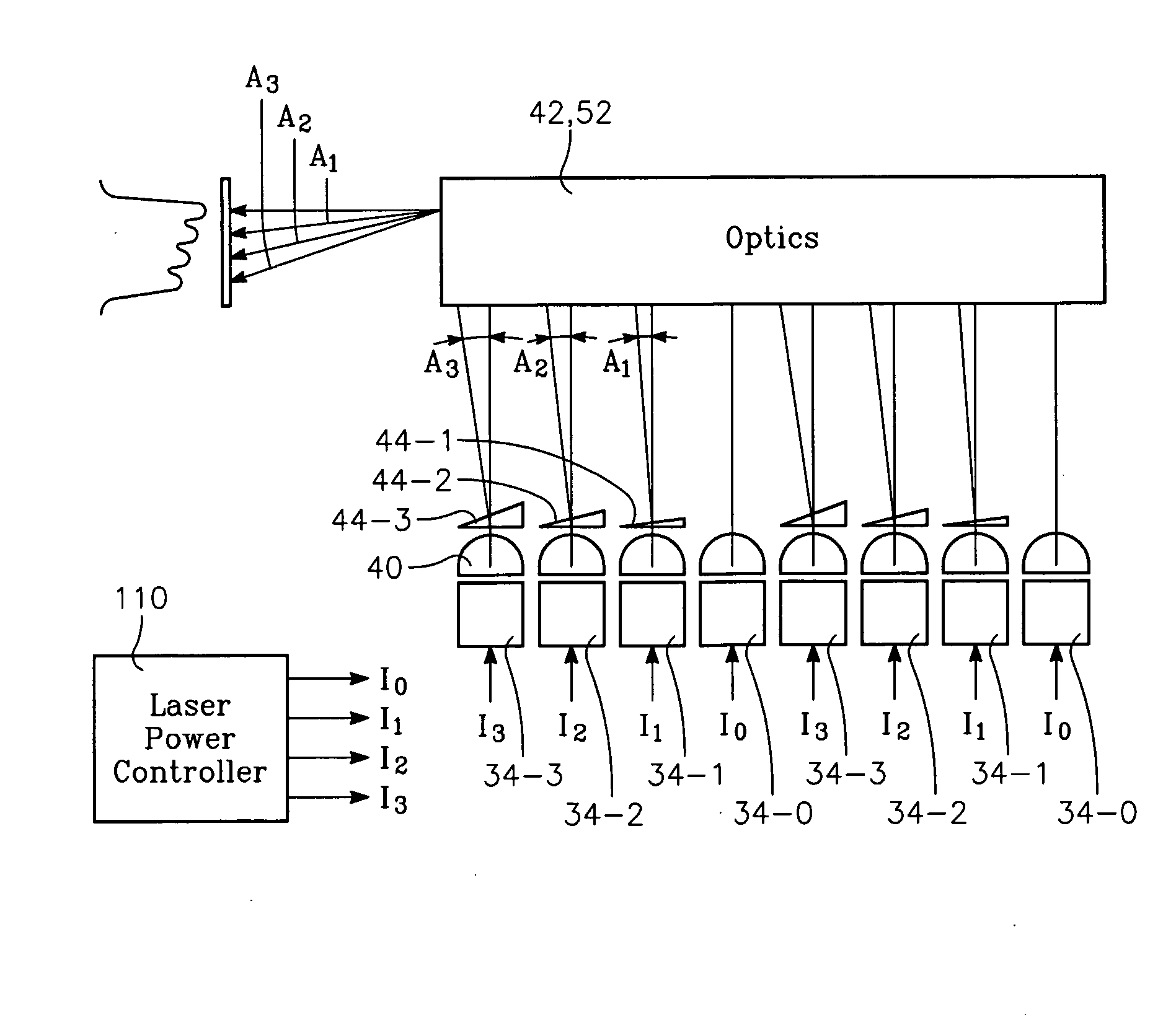
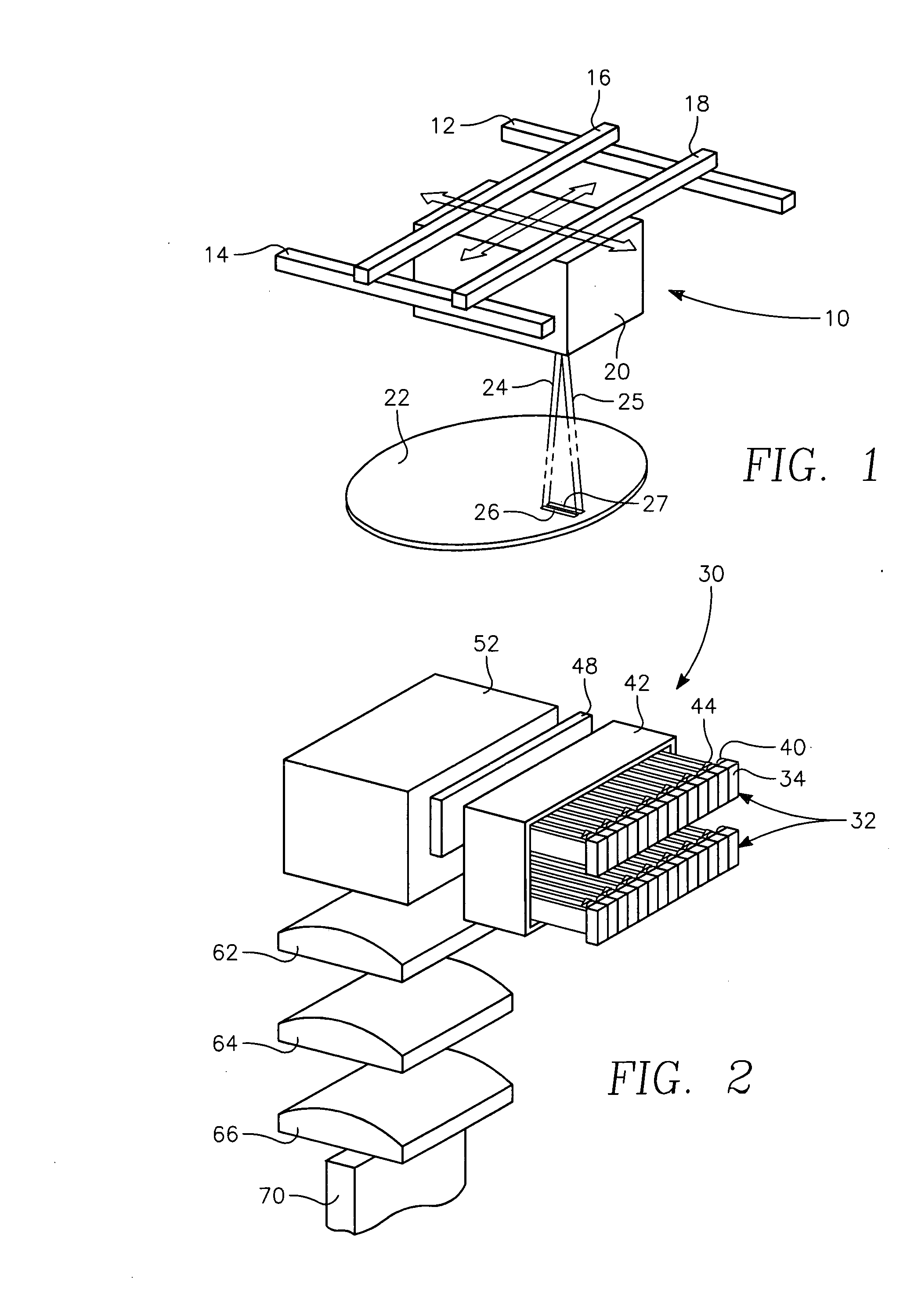
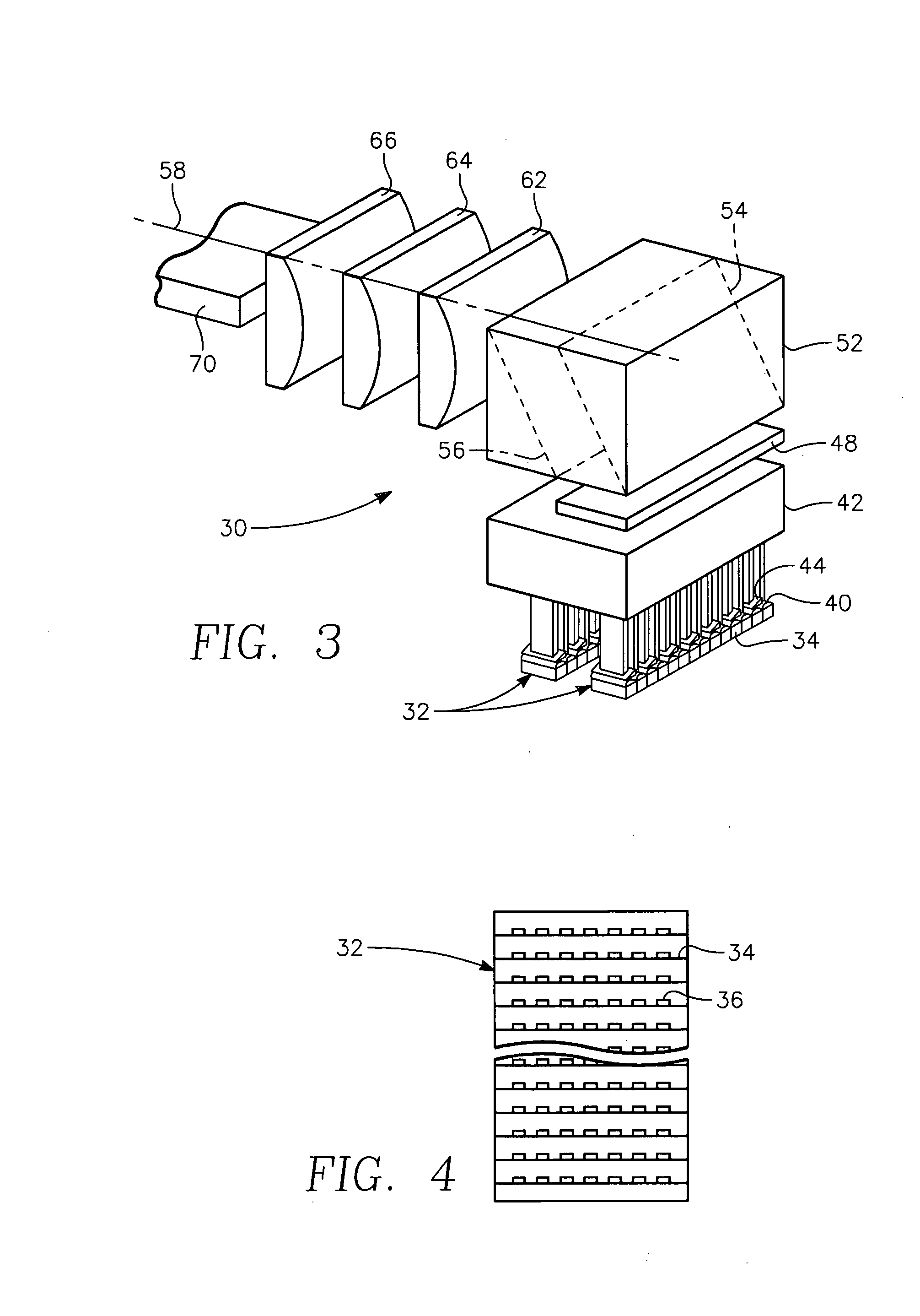
[0031]Defects in an ion implanted wafer of the type that persist beyond a half millisecond at high temperature (1300 degrees C.) are annealed or cured by providing a very long dwell time (e.g., 2-3 milliseconds) without compromising the extremely steep rising and falling edges of the Gaussian shaped line beam along the fast axis. In this way, boundary defects that are an artifact of pre-implant amorphization and post implant annealing are completely removed without incurring a corresponding penalty in thermal diffusion. All this is accomplished by focusing a first set of lasers on a first line beam image and focusing a second set of lasers on a second line beam image whose amplitude peak is displaced from the amplitude peak of the first line beam image along the direction of the fast axis (i.e., perpendicular to the length of the line beam). This displacement is preferably the width of the Gaussian profile of the line beam along the fast axis at an amplitude correspondi...


PUM

PropertyMeasurementUnit
optical deflection angleaaaaaaaaaa
deflection angleaaaaaaaaaa
currentaaaaaaaaaa

Abstract

A dynamic surface anneal apparatus for annealing a semiconductor workpiece has a workpiece support for supporting a workpiece, an optical source and scanning apparatus for scanning the optical source and the workpiece support relative to one another along a fast axis. The optical source includes an array of laser emitters arranged generally in successive rows of the emitters, the rows being transverse to the fast axis. Plural collimating lenslets overlie respective ones of the rows of emitters and provide collimation along the fast axis. The selected lenslets have one or a succession of optical deflection angles corresponding to beam deflections along the fast axis for respective rows of emitters. Optics focus light from the array of laser emitters onto a surface of the workpiece to form a succession of line beams transverse to the fast axis spaced along the fast axis in accordance with the succession of deflection angles.

Description

FIELD OF THE INVENTION[0001]The invention relates generally to thermal processing of semiconductor substrates. In particular, the invention relates to laser thermal processing of semiconductor substrates.BACKGROUND ART[0002]Thermal processing is required in the fabrication of silicon and other semiconductor integrated circuits formed in silicon wafers or other substrates such as glass panels for displays. The required temperatures may range from relatively low temperatures of less than 250 degrees C. to greater than 1400 degrees C. and may be used for a variety of processes such as dopant implant annealing, crystallization, oxidation, nitridation, silicidation, and chemical vapor deposition as well as others.[0003]For the very shallow circuit features required for advanced integrated circuits, it is greatly desired to reduce the total thermal budget in achieving the required thermal processing. The thermal budget may be considered as the total time at high temperatures necessary to ...

Claims


Application Information

Patent Timeline
Patent Type & Authority Applications(United States)
IPC IPC(8): B23K26/00
CPCB23K26/0613B23K26/0676Y10T117/1016H01L21/268H01L29/7833B23K26/0738
Inventor JENNINGS, DEANMAYUR, ABHILASH J.THOMAS, TIMOTHY N.PARIHAR, VIJAYACHUTHARAMAN, VEDAPURAM S.THAKUR, RANDHIR P. S.
Owner APPLIED MATERIALS INC
Why Eureka
Try Eureka