Wafer holder, heater unit used for wafer prober and having wafer holder, and wafer prober

Inactive Publication Date: 2008-09-04
SUMITOMO ELECTRIC IND LTD
View PDF2 Cites 339 Cited by
  • Summary
  • Abstract
  • Description
  • Claims
  • Application Information

AI Technical Summary

Benefits of technology

[0012]The present invention was made to solve the above-described problems, and its object is to provide a wafer holder hardly deformable even under high load and capable of effectively preventing contact failure, and capable of preve

Problems solved by technology

Therefore, when the chuck top is thin, the chuck top might possibly be deformed, resulting in contact failure between the semiconductor wafer and a probe pin.
When such a thick metal plate is used, however, it takes long time to increase and decrease temperature of the semiconductor wafer, which is a significant drawback in improving the throughput.
Consequently, it is impossible by the technique disclosed in Patent Document 1 only to sufficiently suppress deformation of the wafer holder at the time of measuring e

Method used


Image

  • Wafer holder, heater unit used for wafer prober and having wafer holder, and wafer prober
  • Wafer holder, heater unit used for wafer prober and having wafer holder, and wafer prober
  • Wafer holder, heater unit used for wafer prober and having wafer holder, and wafer prober

Examples


example 1

[0118]Ten wafer holders in accordance with the present invention and one wafer holder as a comparative example as listed in Table 1 were fabricated. These wafer holders were each mounted on a wafer prober, and semiconductors were inspected under seven different inspection conditions as shown in Table 2. Respective wafer holders will be described in the following.

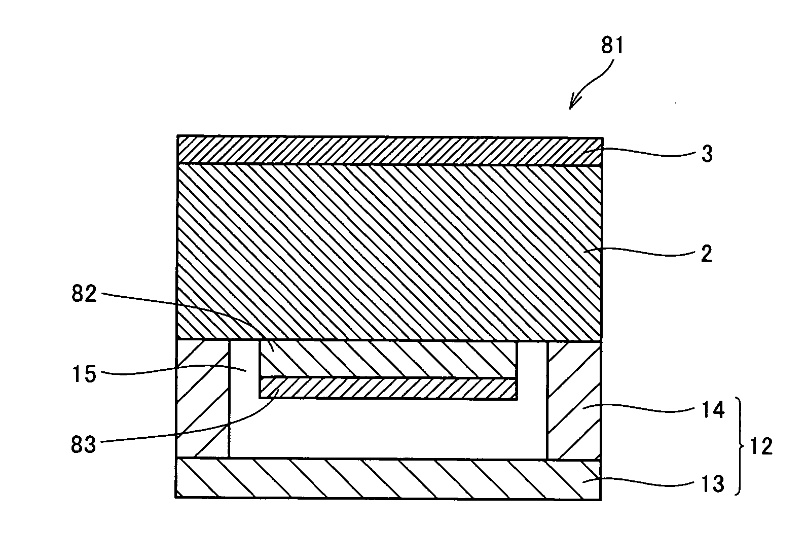
[0119]Wafer holder 31 as the example shown in FIG. 6 was fabricated. As chuck top 2, an Si—SiC substrate having the diameter of 310 mm and thickness of 15 mm was prepared. On one surface of the substrate, a trench in a concentrical circle for vacuum-chucking a wafer and a through hole were formed, and nickel plating was applied as the chuck top conductive layer, whereby the wafer-mounting surface was prepared. Thereafter, the wafer-mounting surface was polished and finished to have the overall warp of 10 μm and surface roughness Ra of 0.02 μm, and chuck top 2 was completed.

[0120]Thereafter, as supporter 33, an Al—SiC plate h...

example 2

[0125]A wafer holder was fabricated in the similar manner as in Example 1 except that the surface to be in contact with the chuck top and the bottom surface of the supporter were finished to the flatness of 0.05 mm, and mounted on a wafer prober, and semiconductors were inspected continuously for 10 hours, under seven different inspection conditions shown in Table 2.

example 3

[0126]A wafer holder was fabricated in the similar manner as in Example 1 except that the surface to be in contact with the chuck top and the bottom surface of the supporter were finished to the flatness of 0.009 mm, and mounted on a wafer prober, and semiconductors were inspected continuously for 10 hours, under seven different inspection conditions shown in Table 2.


PUM


Abstract

By wafer holder including a chuck top for mounting a wafer and a supporter supporting the chuck top and having flatness of at most 0.1 mm, a heater unit for a wafer prober and the wafer prober using the wafer holder, a wafer holder and a wafer prober apparatus hardly deformable even under high load and capable of effectively preventing contact failure, and capable of preventing temperature increase in a driving system when a semiconductor wafer having semiconductor chips with minute circuitry that requires high accuracy is heated can be provided. In the wafer holder of the present invention, the flatness of the supporter is preferably at most 0.05 mm, and more preferably at most 0.01 mm.

Description

BACKGROUND OF THE INVENTION[0001]1. Field of the Invention[0002]The present invention relates to a wafer holder and a heater unit used for a wafer prober in which a semiconductor wafer is mounted on a wafer-mounting surface and a probe card is pressed onto the wafer for inspecting electric characteristics of the wafer, as well as to a wafer prober having these mounted thereon.[0003]2. Description of the Background Art[0004]Conventionally, in the step of inspecting a semiconductor wafer, the semiconductor wafer as an object of processing is subjected to heat treatment. Here, burn-in process is performed in which the semiconductor wafer is heated to a temperature higher than the temperature of normal use, to accelerate degradation of a possibly defective semiconductor chip and to remove the defective chip, in order to prevent defects after shipment.[0005]In the burn-in process, before cutting the semiconductor wafer having circuits formed thereon into individual semiconductor chips, e...

Claims


Application Information

Patent Timeline
IPC IPC(8): G01R31/02B23B5/22
CPCG01R31/2865G01R31/2875Y10T279/17H01L21/68757H01L21/67109
Inventor SHINMA, KENJIITAKURA, KATSUHIROAWAZU, TOMOYUKINAKATA, HIROHIKO
Owner SUMITOMO ELECTRIC IND LTD
Why Eureka
Try Eureka