Charged particle beam writing apparatus and charged particle beam writing method

a writing apparatus and charge technology, applied in the field of charged particle beam writing apparatus and charged particle beam writing method, can solve the problems of large error, affecting the dimension error of a pattern, and adding the position error of two shots on both sides as an error factor, so as to achieve the effect of reducing the dimension error

Inactive Publication Date: 2008-09-11
NUFLARE TECH INC
View PDF5 Cites 14 Cited by
  • Summary
  • Abstract
  • Description
  • Claims
  • Application Information

AI Technical Summary

Benefits of technology

[0026]An object of the invention is to provide a writing apparatus that causes a decrease in dimension error even for pattern formation in which a portion where a resist is left is made a pattern and a writing method using the device.

Problems solved by technology

If a pattern is formed by one shot, as described above, only an error of shaping deflection will affect a dimension error of a pattern.
However, when patterns leaving a resist are formed, left and right patterns are written by a writing apparatus and thus, position errors of two shots on both sides will further be added as an error factor.
When the positive type resist 361 is used and a pattern is formed by leaving a resist, as described above, there has been a problem that, in addition to a forming error component √{square root over ( )}(δl12), further a position error component √{square root over ( )}(12>+22>) is included, leading to a large error.
However, using two types of resist has caused many problems shown below.
First, using two types of resist in one process has complicated maintenance and management of the process.
As a result, problems such as an operational error being more likely to be invited have been caused.
Moreover, an increase in maintenance costs of the line thereof has resulted.
As a result, problems such as being a factor of cost increases of a semiconductor apparatus have been caused.
Second, when a negative type resist is used, there has been a problem of swelling and also a problem of difficulty of forming a finer pattern.
Thus, there has been a problem that it will be difficult to form a pattern as patterns become increasingly more microscopic in the future.
Also, there has been a problem for some type of negative type chemically amplified resist to be more likely to cause waste, creating a problem of causing yield deterioration during pattern formation.
Thus, there is a problem of damage to the transistor.
As has been described above, there has been a problem that a dimension error is large for pattern formation in which a positive type resist is used and a portion where a resist is removed is made a pattern.
If a negative type resist is used, on the other hand, there has been a problem that other problems described above are caused.

Method used


Image

  • Charged particle beam writing apparatus and charged particle beam writing method
  • Charged particle beam writing apparatus and charged particle beam writing method
  • Charged particle beam writing apparatus and charged particle beam writing method

Examples


embodiment 1

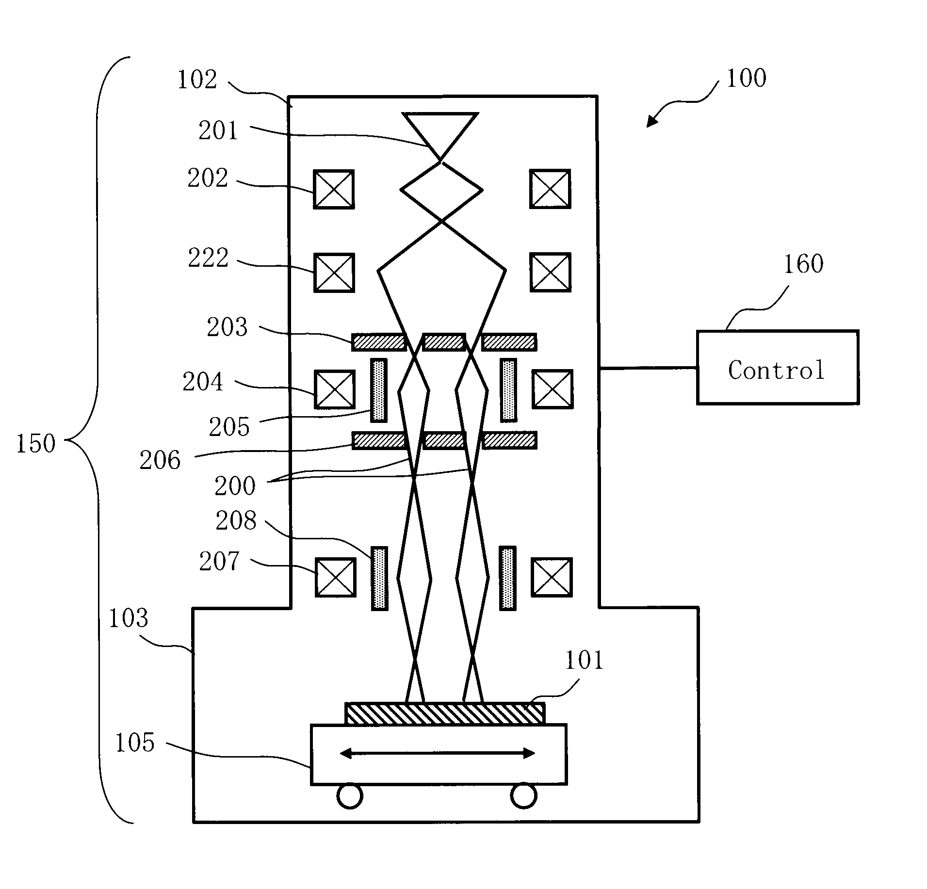
[0063]FIG. 1 is a conceptual diagram exemplifying the principal part configuration of a writing apparatus in the first embodiment.

[0064]In FIG. 1, a writing apparatus 100 is an example of a charged particle beam writing apparatus. The writing apparatus 100 writes, or “draws” a predetermined pattern on a target workpiece 101. The writing apparatus 100 comprises a writing part 150 and a control part 160. The writing part 150 has an electron lens barrel 102 and a writing chamber 103. Inside the electron lens barrel 102, an electron gun 201, an illuminating lens 202, a projecting lens 222, a first shaping aperture plate 203 (an example of an aperture member), a projecting lens 204, a shaping deflector 205 (an example of a deflection part), a second shaping aperture plate 206 (an example of an aperture member), an objective lens 207, and a position deflector 208 are arranged. The electron gun 201 is an example of an irradiation part. An XY stage 105 movably arranged is arranged inside th...

embodiment 2

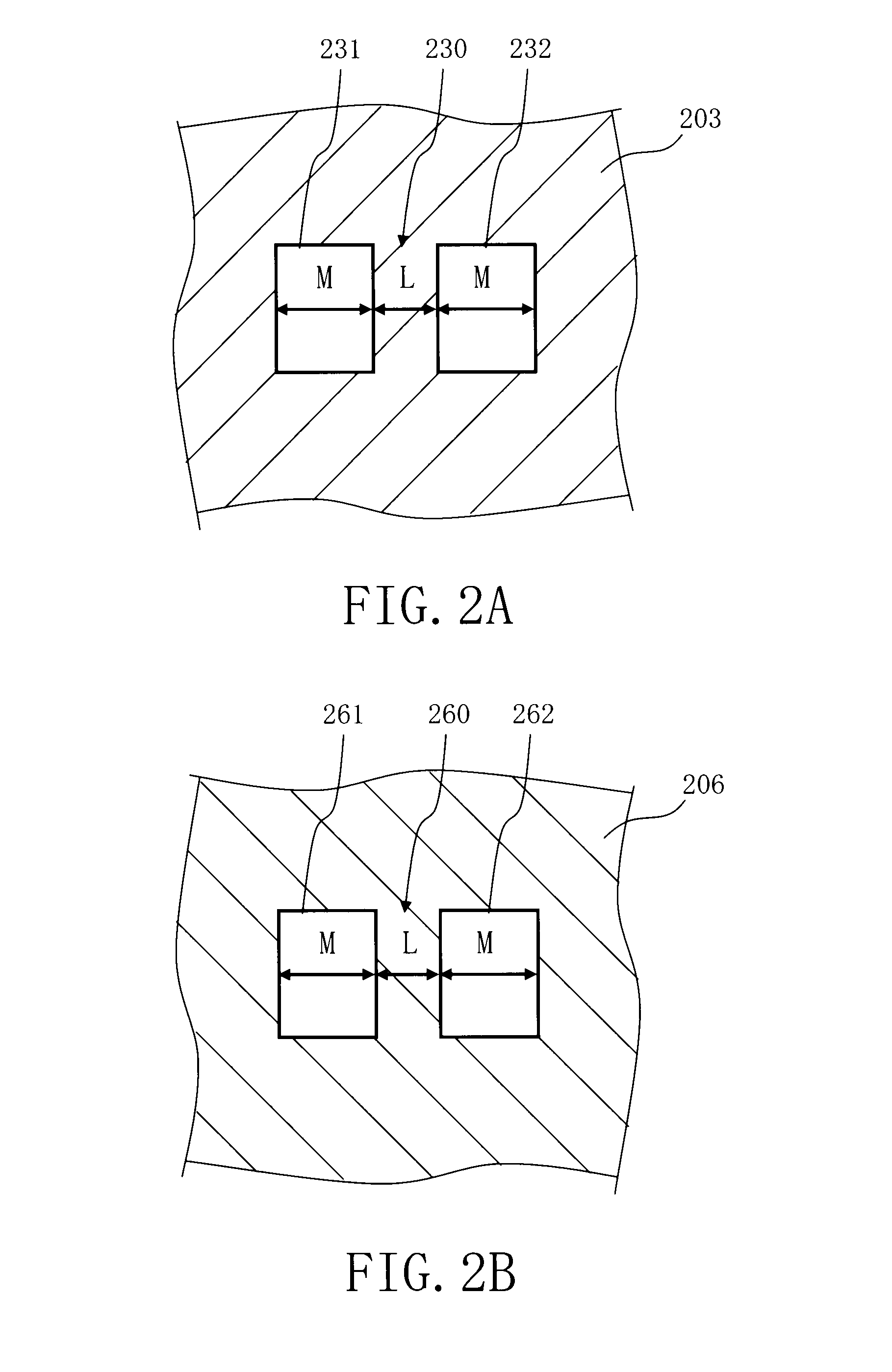
[0095]In the first embodiment, a case in which the shape of an area sandwiched by two patterns formed on the target workpiece 101 by passage of a charged particle beam through openings of the first and second shaping aperture members and by which a charged particle beam is blocked has a linear shape without changing its direction at some midpoint has been described. However, the present invention is not limited to this. In a second embodiment, a case in which the shape of an area sandwiched by two patterns formed on the target workpiece 101 by passage of a charged particle beam through openings of the first and second shaping aperture members and by which a charged particle beam is blocked changes its direction at some midpoint will be described. The second embodiment is the same as the first embodiment except the shapes of openings formed in the first shaping aperture member 203 and those formed in the second shaping aperture member 206.

[0096]FIG. 19A and FIG. 19B are diagrams show...


PUM


Abstract

A charged particle beam writing apparatus includes an irradiation part configured to irradiate a charged particle beam; a first shaping aperture member having passing areas, that the charged particle beam passes through, on both sides of an area blocking the charged particle beam; a deflection part configured to deflect the charged particle beam that has passed through the first shaping aperture member; a second shaping aperture member having passing areas, that the charged particle beam passes through, on both sides of an area blocking the deflected charged particle beam; and a stage on which a target workpiece irradiated with the charged particle beam that has passed through the second shaping aperture member is placed.

Description

CROSS-REFERENCE TO RELATED APPLICATION[0001]This application is based upon and claims the benefit of priority from prior Japanese Patent Application No. 2007-060826 filed on Mar. 9, 2007 in Japan, the entire contents of which are incorporated herein by reference.BACKGROUND OF THE INVENTION[0002]1. Field of the Invention[0003]The invention relates to a charged particle beam writing apparatus and a charged particle beam writing method, and in particular, relates to an electron beam writing apparatus featuring two aperture shapes and an electron beam writing method of writing using the device.[0004]2. Related Art[0005]Lithography technology assuming the role of advancement for still finer semiconductor devices is, among semiconductor manufacturing processes, an extremely important process to solely generate patterns. In recent years, with ever higher integration of LSI, the circuit line width demanded for semiconductor devices is becoming finer year by year. To form circuit patterns de...

Claims


Application Information

Patent Timeline
Patent Type & Authority Applications(United States)
IPC IPC(8): H01J37/30H01J3/26
CPCB82Y10/00B82Y40/00H01J2237/0453H01J37/09H01J37/3174G03F1/20
Inventor ABE, TAKAYUKI
Owner NUFLARE TECH INC
Why Eureka
Try Eureka