Metal e-Fuse structure design

Active Publication Date: 2008-09-11
TAIWAN SEMICON MFG CO LTD
View PDF15 Cites 56 Cited by
  • Summary
  • Abstract
  • Description
  • Claims
  • Application Information

AI Technical Summary

Benefits of technology

[0009]By increasing the pattern density of local fuse regions, metal fuses formed in the local fuse regions may have reduced thicknesses, and t

Problems solved by technology

Thickness T, therefore, cannot be customized to satisfy the requir

Method used


Image

  • Metal e-Fuse structure design
  • Metal e-Fuse structure design
  • Metal e-Fuse structure design

Examples


Example

[0014]The making and using of the presently preferred embodiments are discussed in detail below. It should be appreciated, however, that the present invention provides many applicable inventive concepts that can be embodied in a wide variety of specific contexts. The specific embodiments discussed are merely illustrative of specific ways to make and use the invention, and do not limit the scope of the invention.

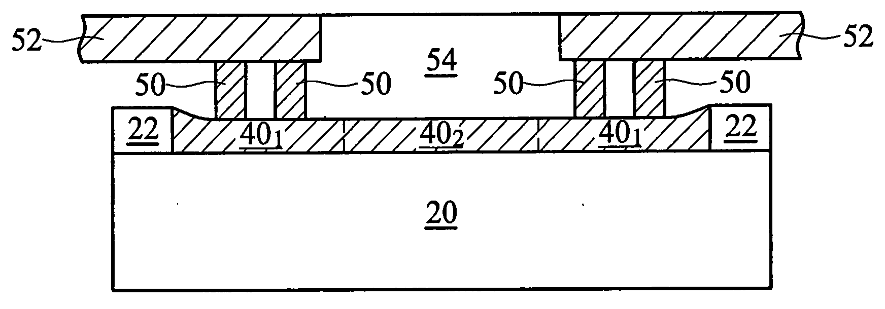
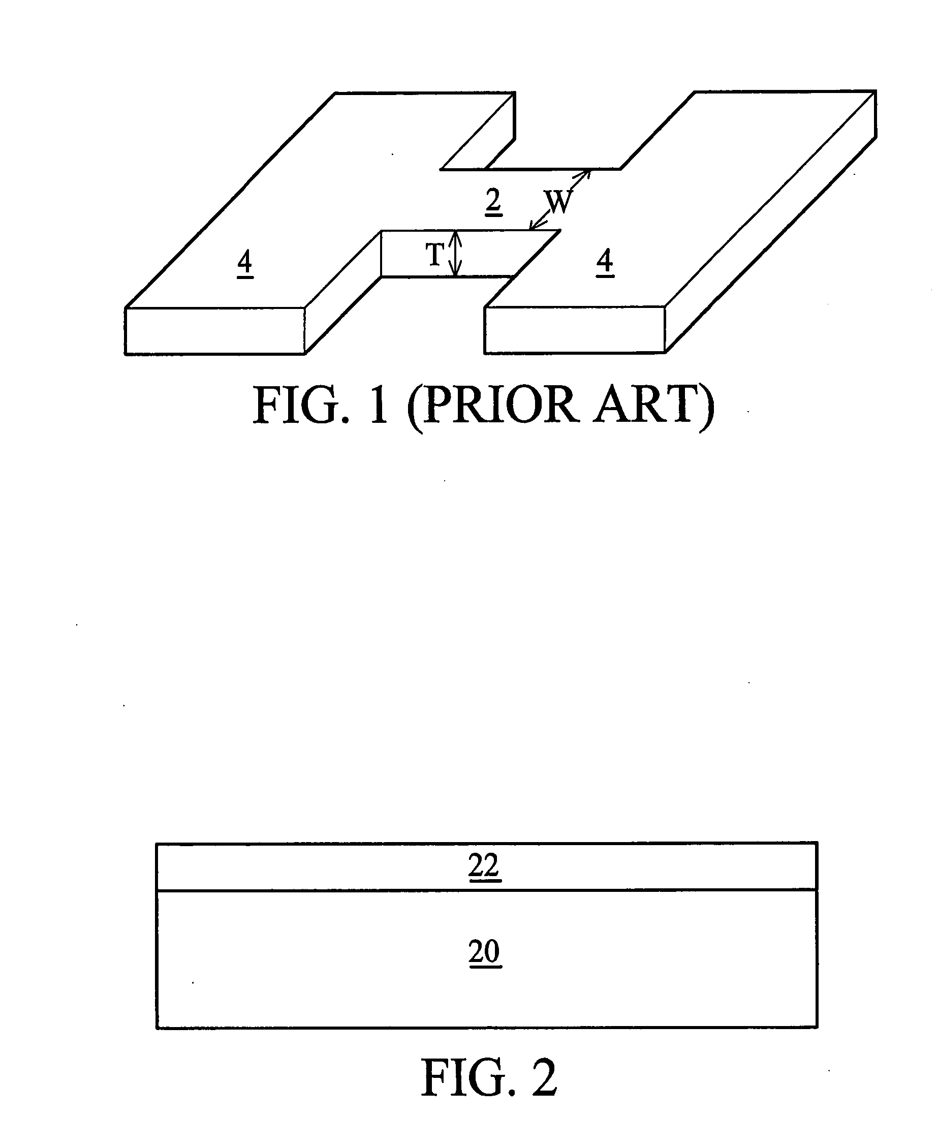
[0015]FIG. 2 illustrates a starting structure, which includes a schematically illustrated base layer 20 and overlying dielectric layer 22. Base layer 20 may include a semiconductor substrate (not shown). Other layers, such as a contact etch stop layer, an inter-layer dielectric, and an inter-metal dielectrics (not shown), may also be included in base layer 20. The semiconductor substrate may be a single crystalline or a compound semiconductor substrate. Active devices (not shown) such as transistors may be formed on the semiconductor substrate. In an embodiment, redundant cir...


PUM


Abstract

An integrated circuit structure is provided. The integrated circuit structure includes a semiconductor substrate; a dielectric layer over the semiconductor substrate; a metal fuse in the dielectric layer; a dummy pattern adjacent the metal fuse; and a metal line in the dielectric layer, wherein a thickness of the metal fuse is substantially less than a thickness of the metal line.

Description

TECHNICAL FIELD[0001]This invention relates generally to semiconductor structures, and more particularly to electrical fuses and a fabrication method thereof.BACKGROUND[0002]In the semiconductor industry, fuse elements are widely used in integrated circuits for a variety of purposes, such as improving manufacturing yield or customizing generic integrated circuits. For example, by replacing defective circuits on a chip with duplicate or redundant circuits on the same chip, manufacturing yields can be significantly increased. A fuse disconnected by a laser beam is referred to as a laser fuse, while a fuse disconnected by passing an electrical current, or blowing, is referred to as an electrical fuse, or e-Fuse. By selectively blowing fuses within an integrated circuit, which has multiple potential uses, a generic integrated circuit design may be economically manufactured and adapted to a variety of customer uses.[0003]Typically, fuses are incorporated in the design of the integrated c...

Claims


Application Information

Patent Timeline
IPC IPC(8): H01L29/00
CPCH01L23/5256H01L2924/0002H01L2924/00
Inventor CHEN, HSIEN-WEITSAI, HAO-YIJENG, SHIN-PUUHSU, SHIH-HSUN
Owner TAIWAN SEMICON MFG CO LTD
Why Eureka
Try Eureka