

Method of forming contact plugs for eliminating tungsten seam issue
a technology of contact plugs and tungsten seams, which is applied in the direction of electrical equipment, semiconductor devices, semiconductor/solid-state device details, etc., can solve the problems of electrical device degradation, difficult topology for subsequent metallization coverage, and increased tungsten seam siz
- Summary
- Abstract
- Description
- Claims
- Application Information
AI Technical Summary
Benefits of technology
Problems solved by technology
Method used
Image

Examples
Embodiment Construction
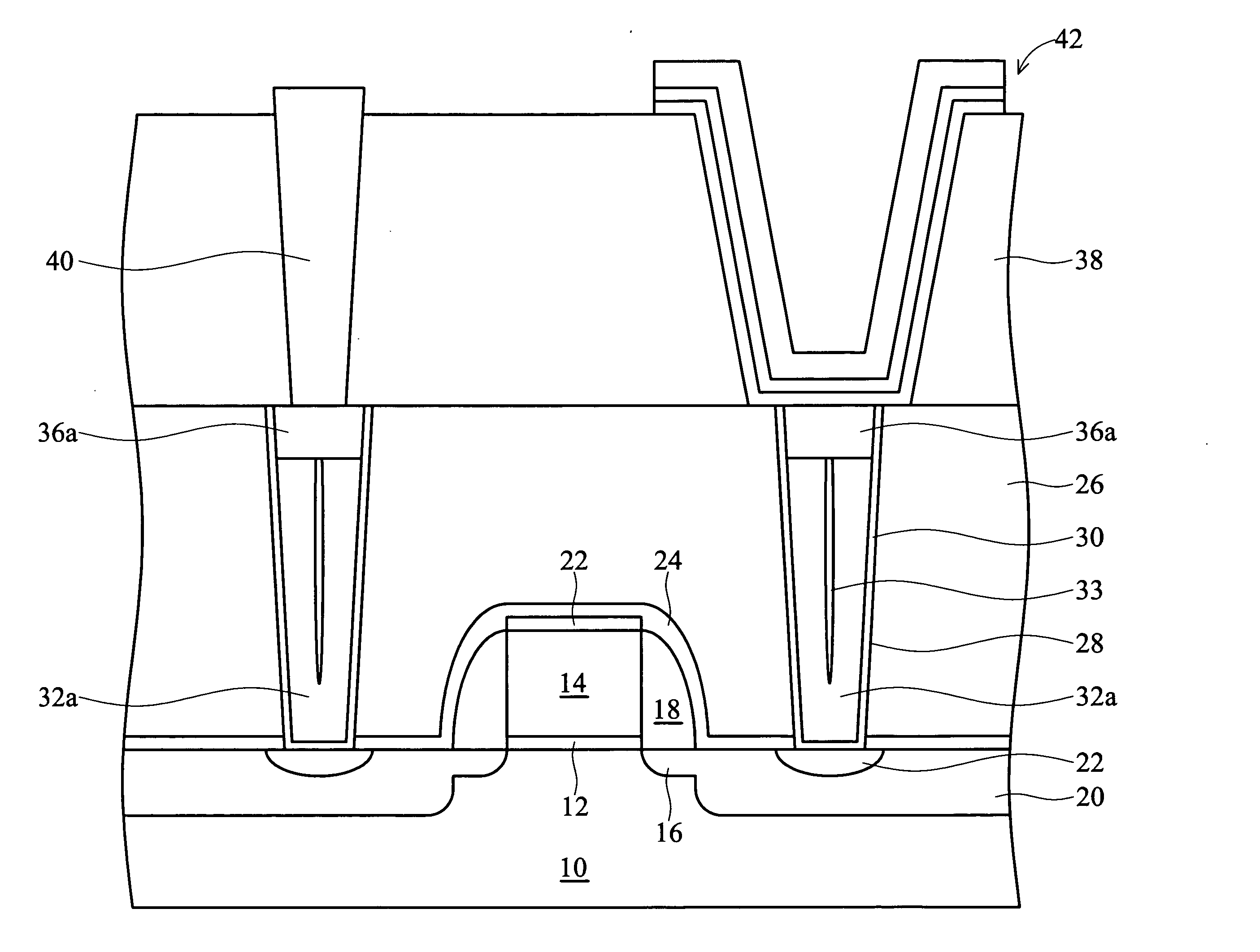
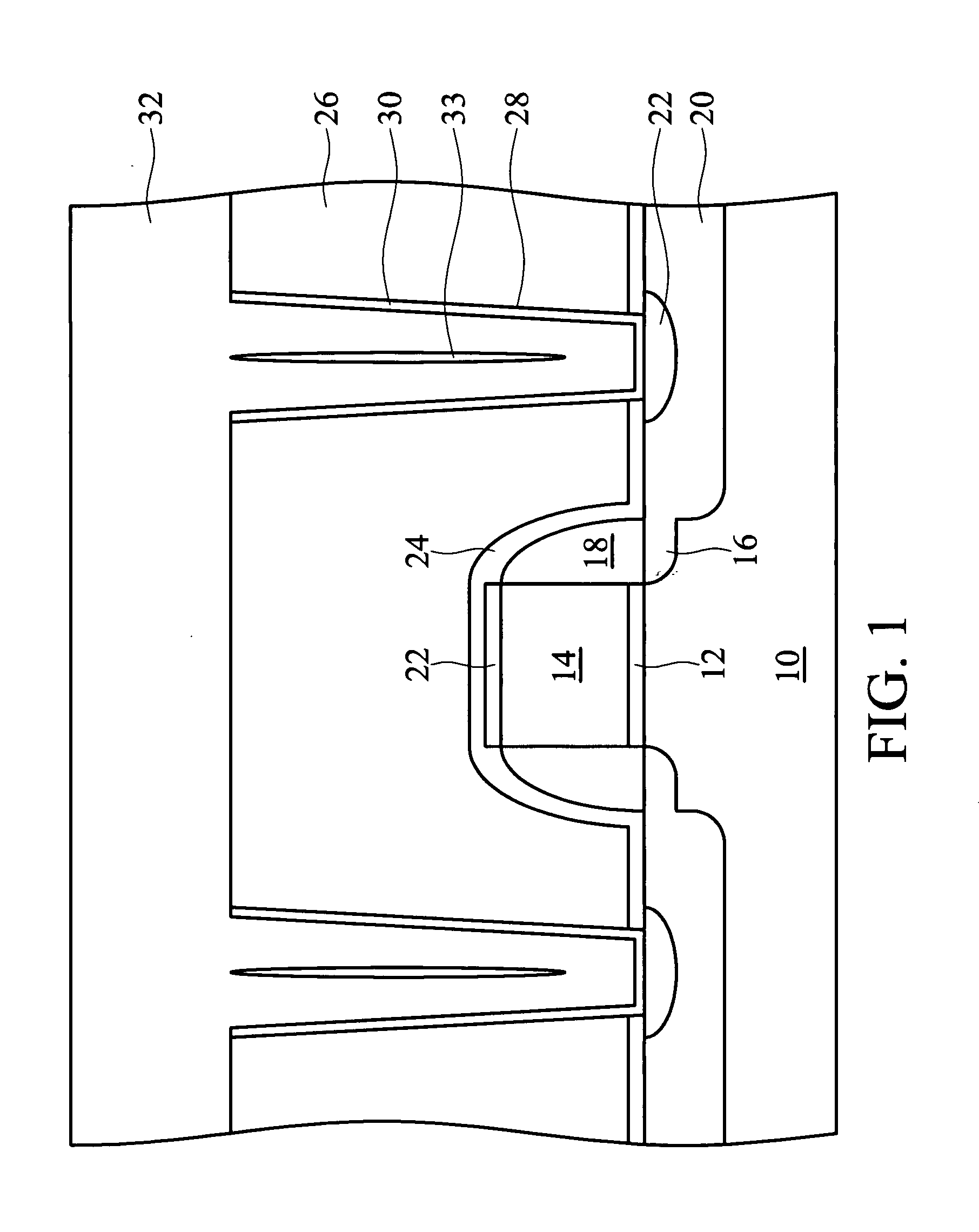
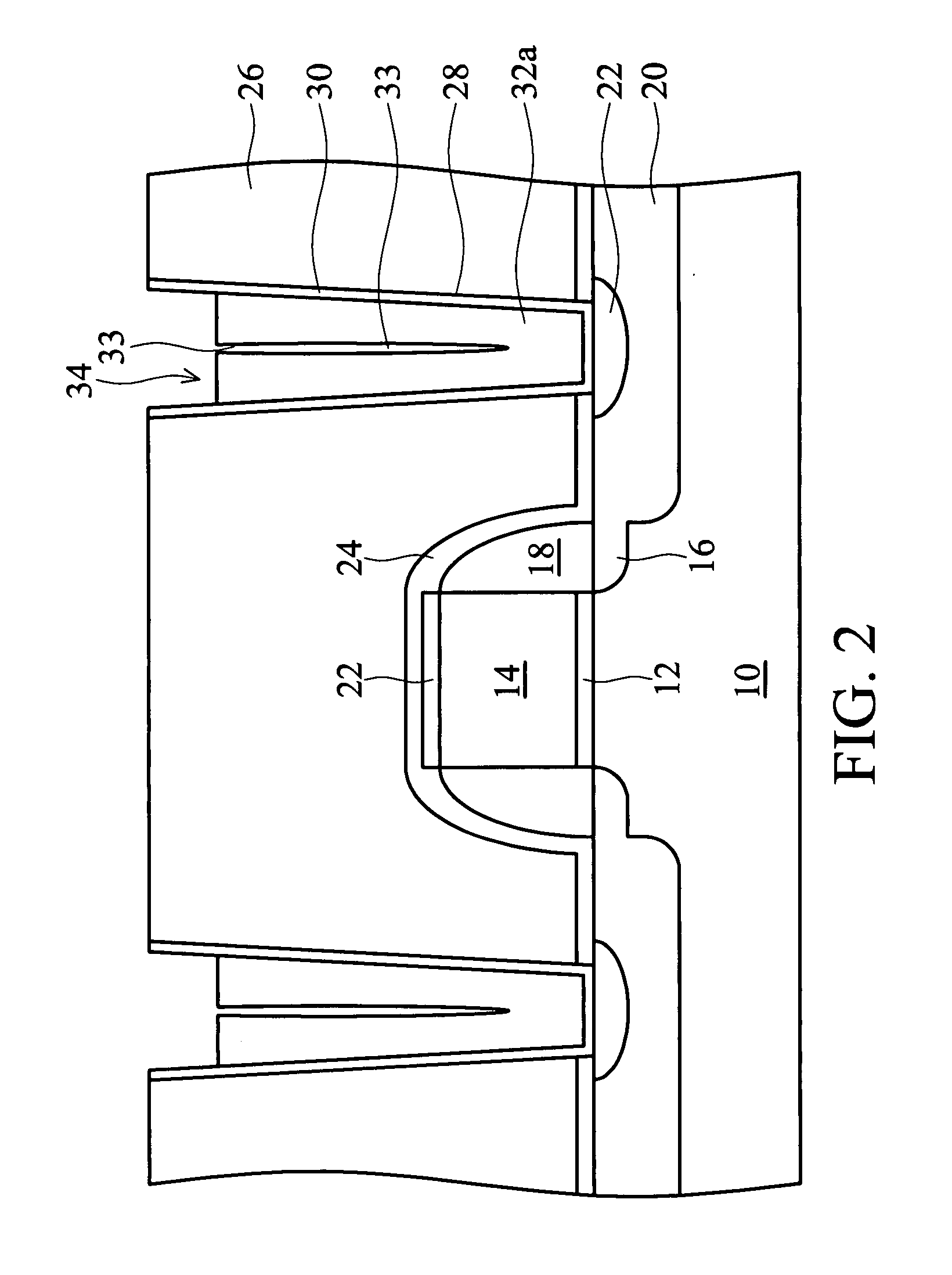
[0008]Embodiments of the present invention provide methods of forming tungsten contact plugs to eliminate tungsten seams. For eDRAM applications, the inventive method can decrease failure bit count to improve device yield. Reference will now be made in detail to the present embodiments, examples of which are illustrated in the accompanying drawings. Wherever possible, the same reference numbers are used in the drawings and the description to refer to the same or like parts. In the drawings, the shape and thickness of one embodiment may be exaggerated for clarity and convenience. This description will be directed in particular to elements forming part of, or cooperating more directly with, apparatus in accordance with the present invention. It is to be understood that elements not specifically shown or described may take various forms well known to those skilled in the art. Further, when a layer is referred to as being on another layer or “on” a substrate, it may be directly on the o...
PUM
| Property | Measurement | Unit |
|---|---|---|
| depth | aaaaa | aaaaa |
| thickness | aaaaa | aaaaa |
| thickness | aaaaa | aaaaa |
Abstract
Description
Claims
Application Information