Nanotube array ballistic light emitting devices

Inactive Publication Date: 2008-09-11
NANO ELECTRONICS & PHOTONIC DEVICES & CIRCUITS
View PDF21 Cites 13 Cited by
  • Summary
  • Abstract
  • Description
  • Claims
  • Application Information

AI Technical Summary

Benefits of technology

[0011]To build a nanotube array ballistic photonic devices according to the present invention, one has to provide two contacts to each nanotube in the array. Unlike the designs for the transistors described in the above cited U.S. Pat. No. 7,102,157, the photonic devices need only two contacts, and no electron emission into vacuum is considered. The first contact is made as a metal electrode deposited on an insulating substrate, like a glass. It is followed

Problems solved by technology

In this configuration, parallel placement of multiple identical nanotubes to enhance the outp

Method used


Image

  • Nanotube array ballistic light emitting devices
  • Nanotube array ballistic light emitting devices
  • Nanotube array ballistic light emitting devices

Examples


Embodiment Construction
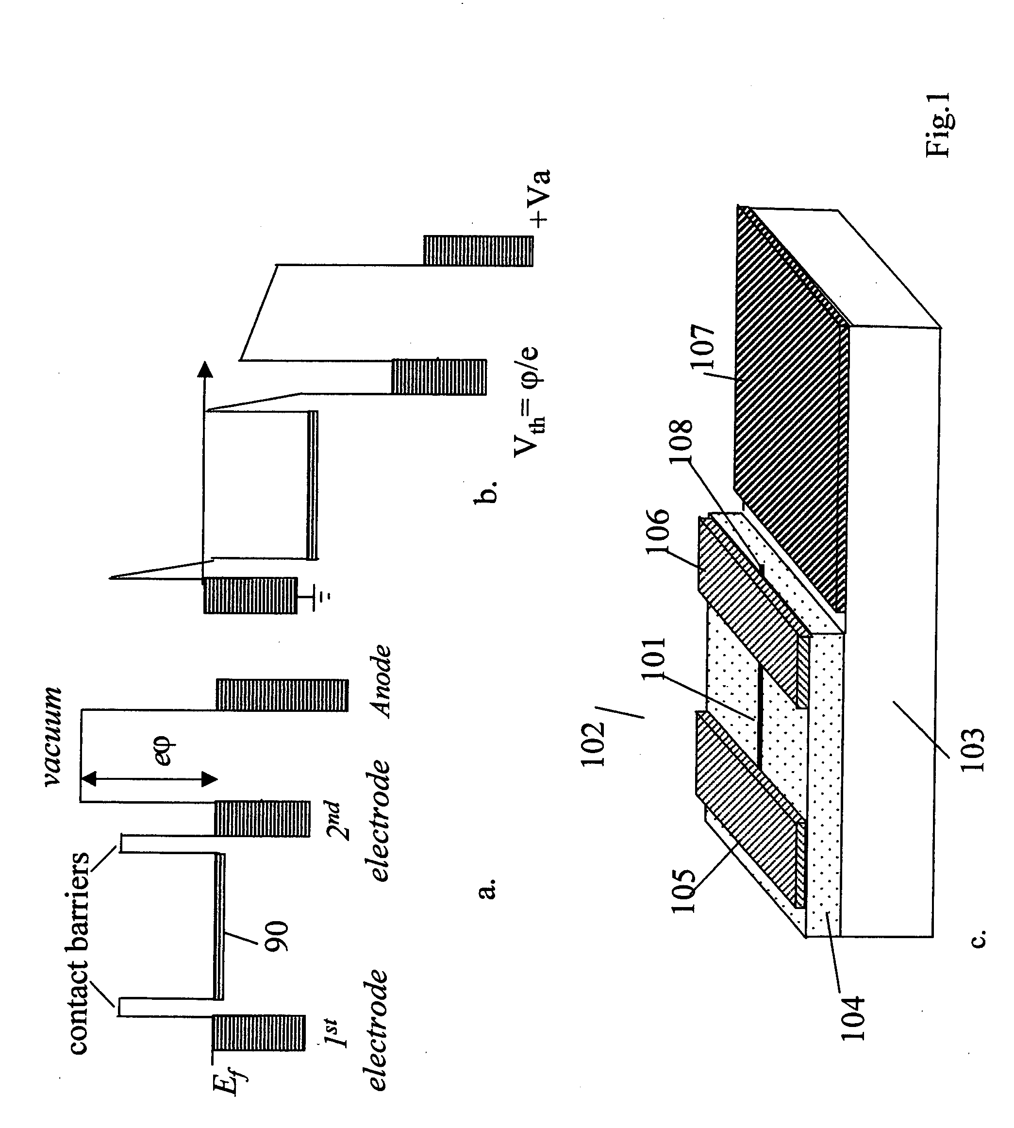
1. The BLED

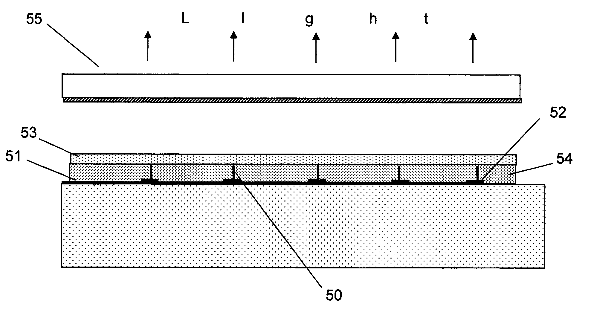
[0017]FIG. 3 shows the cross-sectional view of the BLED structure. The device is made on the insulating substrate (glass) 31. The first metal layer 32 deposited on the substrate serves as a cathode electrode, on which the nanotube array will be grown. The layer 32 will also be used as a mirror to reflect light into upper hemisphere and hence should possess a high optical reflectivity, like Al. Furthermore, since the metal 32 is designed to be the output contact in the BLED, it is preferable to deposit pads of the Pd layer 36, see e.g. A. Javey et al, Nature, 424, 654, 2003, on the metal layer 32 to minimize the contact resistance. Before the nanotube growth, small pads of catalytic material (not shown), such as Ni, Fe or Co, are deposited on the Pd pads to activate the process of growth of the nanotube array 33. It is followed by depositing of an insulator 34, such as SiO2 or SiOx, having the thickness smaller than the nanotube height, and then polishing the top surface t...


PUM


Abstract

A new class of light emitting and laser diodes is disclosed wherein ballistic (without collisions) electron propagation along the nanotubes, grown normally to the substrate plane on the common metal electrode, provides conditions for the light emission from the nanotubes. The electrons, tunneling from the input contact into high energy states in the nanotubes, emit light via electron energy relaxation between the quantum energy levels existing in the nanotubes due to quantum size effect.
In the disclosed devices, planar layer deposition technology is used to form a diode structure with two electrodes attached to the nanotubes ends.

Description

FIELD OF THE INVENTION[0001]The invention relates to carbon nanotube-based ballistic opto-electronic devices, in particular, light emitting diodes and lasers employing array of grown nanotubes.BACKGROUND OF THE INVENTION[0002]The carbon nanotubes (CNT) possess unique properties due to extremely small nanotube diameter (˜1 nm for a single walled nanotube, SWNT) which gives rise to a strong two-dimensional quantization of the energy spectrum. As a result, the electron scattering is largely suppressed and the electrons move along the nanotube ballistically, i.e. without collisions and loss of energy, while the nanotube resistance is essentially controlled by the contact resistances. The minimum contact resistance is determined by the quantum contact resistance of 6.5 kOhm (per contact).[0003]In the previous patent U.S. Pat. No. 7,102,157, the ballistic electron propagation along the nanotube was utilized to disclose a vacuum electron emitter, in which electrons under the potential diff...

Claims


Application Information

Patent Timeline
IPC IPC(8): H01J1/62
CPCB82Y20/00H01L33/18H01S5/0425H01S5/3415H01S5/30H01S5/3027H01S5/183Y10S977/932Y10S977/70H01S5/04253
Inventor KASTALSKY, ALEXANDER
Owner NANO ELECTRONICS & PHOTONIC DEVICES & CIRCUITS
Why Eureka
Try Eureka