Probe fed patch antenna

a patch antenna and antenna technology, applied in the direction of resonant antennas, substantially flat resonant elements, radiating element structural forms, etc., can solve the problems of increasing the thickness of the antenna, increasing the lateral size of the antenna, and the device's relatively narrow bandwidth, so as to reduce the complexity and cost of elements, improve manufacturability, and reduce mechanical/electrical complexity.

Active Publication Date: 2008-09-11
LOCKHEED MARTIN CORP
View PDF10 Cites 44 Cited by
  • Summary
  • Abstract
  • Description
  • Claims
  • Application Information

AI Technical Summary

Benefits of technology

[0006]The present antenna employs a configuration where no input electrical impedance matching structure in the input line is required. Thus the number of parts / drawings and associated lifetime costs for drawing support are reduced. The physical feed and element structures of the antenna according to an aspect of the invention substantially reduce the need for tight tolerances on all physical dimensions and corresponding dielectric material properties. Thus, the present antenna configuration reduces both element complexity and cost while improving manufacturability. The reduced mechanical / electrical complexity enables use of larger finite array structures in simulations using 3-dimensional (3D) electromagnetic simulation software.
[0007]A microstrip antenna configuration employs a metallic patch which is positioned on the top surface of a dielectric substrate. The dielectric substrate has the bottom surface coated with a suitable metal to form a ground plane. A hole is formed through the ground plane, through the dielectric to allow access to the bottom surface of the patch. A center conductor of a coaxial cable is directly connected to the patch. The center conductor of the coaxial cable is surrounded by a metallic housing within the substrate area. Thus, the probe length is reduced by retaining a coaxial transmission line within the substrate. The patch forms a first plate for the capacitance while the diameter of the coaxial cable outer housing within the substrate is increased to form another plate on the end of the coaxial cable. The value of capacitance can be adjusted by the area of the metallic housing, the relative dielectric constant of material between plates, and the spacing between the plates. The microstrip patch antenna input impedance using the direct probe connection is adjusted and centered at a desired center frequency and many such frequencies can be accommodated.

Problems solved by technology

However, one drawback of such devices is their relatively narrow bandwidth.
However, the antenna substrate supports tightly bound surface wave modes which represent a loss mechanism in the antenna.
However, this has the disadvantage of increasing the thickness of the antenna.
Parasitic patches can also be used in the same layer (coplanar geometry); however, this undesirably increases the lateral size of the antenna and is not suitable for antenna array applications.
As previously mentioned, a disadvantage of microstrip patch antennas which has limited their use is due to their narrow bandwidth and to their inherent nature as resonant devices.
Aperture coupled stacked patch antennas have also been investigated, however, such devices also have certain drawbacks.
This is difficult to provide.
Furthermore, the prior art devices and methods encounter difficulty in meeting required frequency response for many applications.
Still further, such prior art antennas are susceptible to breakdown at high transmission powers.

Method used


Image

  • Probe fed patch antenna
  • Probe fed patch antenna
  • Probe fed patch antenna

Examples


Embodiment Construction

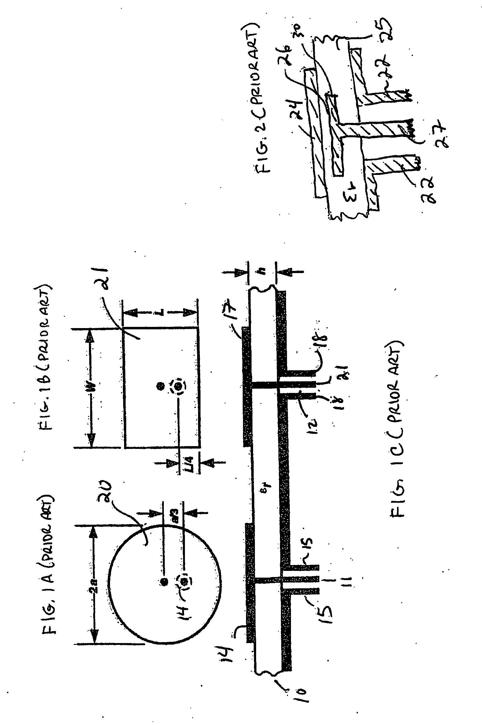
[0020]Before proceeding with the description of the invention, reference is made to FIG. 1, which consists of FIGS. 1a, 1b and 1c. FIGS. 1a, 1b and 1c depict prior art coaxial fed microstrip antennas. Referring to FIG. 1a, there is shown a round or circular microstrip antenna, while FIG. 1b depicts a rectangular microstrip antenna. Although the two most common element configurations are rectangular and round, the antenna itself may be square, rectangular, round, elliptical or other such geometrical shape. The microstrip antenna is well known and for example of such antennas reference is made to the text “Electronic Engineers Handbook 3rd Edition” by D. C. Fink et al. chapter 18 entitled “Antennas and Wave Propagation” pages 18-40 to 18-35. The text shows microstrip antennas and the structures depicted in FIGS. 1a to 1c are taken from that text. See also a text entitled Broadband Microstrip Antennas by G. Kumar & K. P. Ray published by AirTech House (2003). See page 62 depicting seri...


PUM


Abstract

A microstrip antenna configuration employs a metallic patch which is positioned on the top surface of a dielectric substrate. The dielectric substrate has the bottom surface coated with a suitable metal to form a ground plane. A hole is formed through the ground plane, through the dielectric to allow access to the bottom surface of the patch. A center conductor of a coaxial cable is directly connected to the patch. The center conductor of the coaxial cable is surrounded by a metallic housing within the substrate area. The patch forms a first plate for the capacitance while the diameter of the outer housing of the coaxial cable within the substrate is increased to form another plate on the end of the coaxial cable. The value of capacitance can be adjusted by the area of the metallic housing the relative dielectric constant of the spacing material, and the spacing between the plates. The sum of the probe inductive impedance and microstrip patch antenna input impedance using the direct probe connection is adjusted and centered at a desired design center frequency and many such frequencies can be accommodated.

Description

FIELD OF INVENTION[0001]This invention relates generally to antenna configurations and more particularly to a probe-connected patch.BACKGROUND[0002]Microstrip patch antennas have several well known advantages over other antenna structures. These antennas generally have a low profile and conformal nature, are lightweight, have low production cost, are robust in nature and compatible with microwave monolithic integrated circuits (MMICs) and optoelectronic integrated circuits (OEICs) technologies. However, one drawback of such devices is their relatively narrow bandwidth. In order to achieve wider bandwidth, a relatively thick substrate must be used. However, the antenna substrate supports tightly bound surface wave modes which represent a loss mechanism in the antenna. The loss due to surface wave modes increases as the substrate thickness is increased. It is desirable to develop conformal microstip antennas which enjoy wide bandwidth, yet do not suffer from the loss of attractive fea...

Claims


Application Information

Patent Timeline
Patent Type & Authority Applications(United States)
IPC IPC(8): H01Q1/38
CPCH01Q9/045H01Q9/0414H01Q1/38H01Q13/18
Inventor GILLETTE, MARLIN R.
Owner LOCKHEED MARTIN CORP
Why Eureka
Try Eureka