Power Semiconductor Module

a technology of semiconductor modules and semiconductor devices, applied in semiconductor devices, semiconductor/solid-state device details, electrical apparatus, etc., can solve the problems of large thermal resistance that cannot be eliminated, and achieve the effects of reducing heat spreaders, high refrigerating capability, and thermal resistan

Inactive Publication Date: 2008-09-18
HITACHI LTD
View PDF4 Cites 98 Cited by
  • Summary
  • Abstract
  • Description
  • Claims
  • Application Information

AI Technical Summary

Benefits of technology

[0007]According to this invention, a high refrigerating capability can be achieved since the thermal resistance between the power semiconductor chip and the refrigerating means such as a heat spreader c

Problems solved by technology

In the above mentioned structure, the provision of the heat sinks on both sides of the power semiconductor chip indeed enhances the refrigerating performance, but a problem of large thermal resis

Method used


Image

  • Power Semiconductor Module
  • Power Semiconductor Module
  • Power Semiconductor Module

Examples


embodiment 1

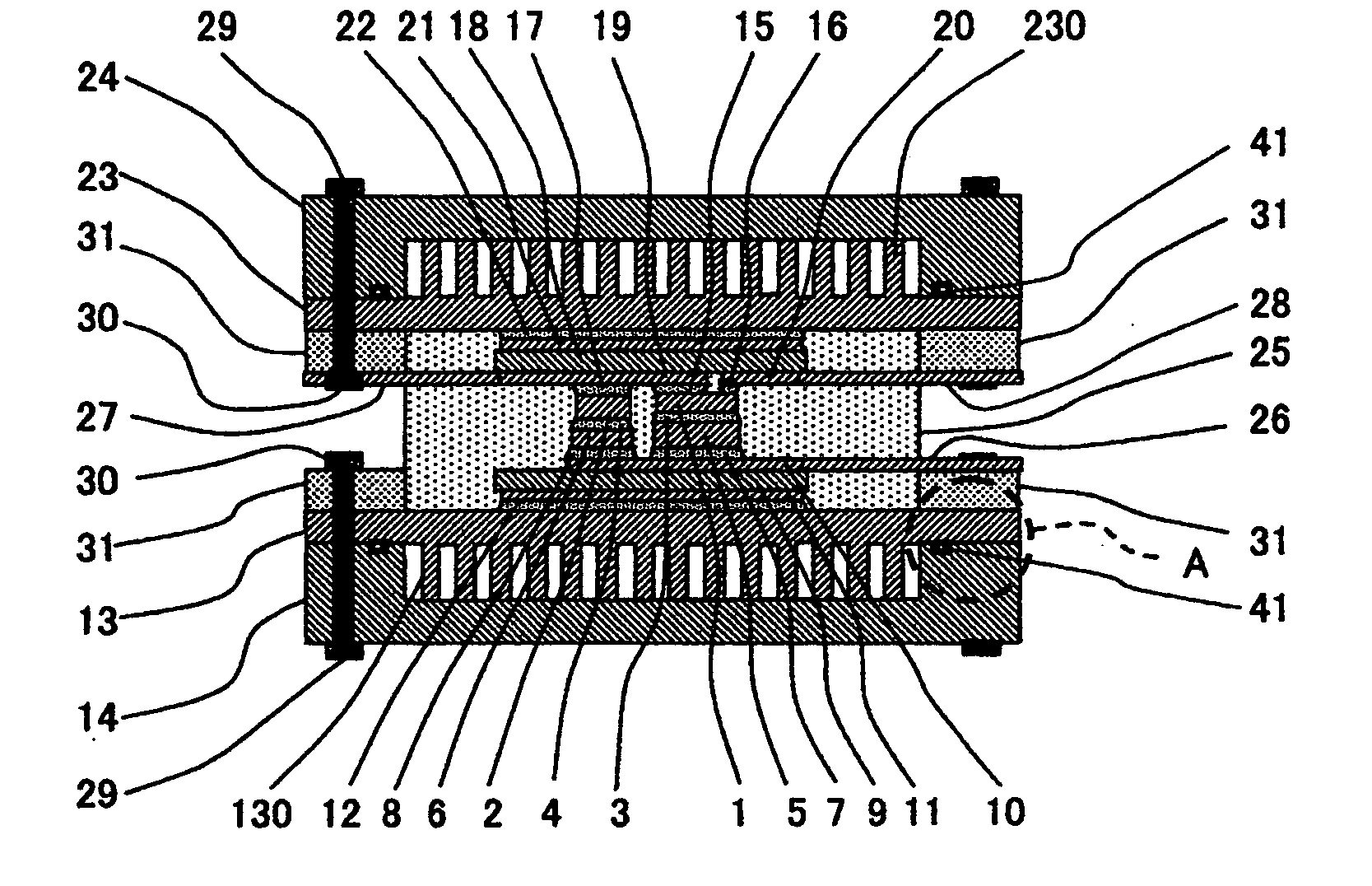
[0035]FIG. 1 schematically shows in vertical cross section a power semiconductor module as a first embodiment of this invention. The power semiconductor module shown in FIG. 1 incorporates therein power semiconductor chips 1, 2 such as insulated gate bipolar transistors (IGBTs) or freewheel diodes. The lower surfaces of the power semiconductor chips 1, 2 are joined to spacers 5, 6 with first joining material layers 3, 4 such as solder in between, respectively.

[0036]The spacers 5, 6 serve to adjust the overall thicknesses of the power semiconductor chips 1, 2 when they are different in thickness from each other. The spacers 4, 5 also serve to prevent electric discharge from taking place between the electrodes 28, 26 provided respectively on the upper and the lower sides of the power semiconductor chip as the insertion of the spacers increases the distance between the electrodes 26, 28. The spacers should preferably have small electric and thermal resistances. Copper, composite materi...

embodiment 2

[0061]FIG. 12 schematically shows in cross section a power semiconductor module as a second embodiment of this invention, the cross section being a vertical cross section perpendicular to the direction of flow of the refrigerant through the refrigerant flow channels. FIG. 13 schematically shows the cross sectional structure of the refrigerant flow channels according to this second embodiment, the cross section being parallel with the direction of flow of the refrigerant.

[0062]A heat sink joined to the lower surface of the lower insulating substrate 9 is similar in structure to that used in the first embodiment described above, wherein the heat spreader 13 with fins 130 erected thereon is covered by the casing 14, and refrigerant flows through the lower flow channels 70 formed in the space enclosed by the heat spreader 13 and the casing 14.

[0063]On the other hand, a heat sink joined to the upper surface of the upper insulating substrate 18 is a thin heat spreader 72 having a single r...

embodiment 3

[0067]FIG. 15 schematically shows in cross section a power semiconductor module as a third embodiment of this invention, the cross section being a vertical cross section perpendicular to the direction of flow of the refrigerant through the refrigerant channels. FIG. 16 schematically shows the cross sectional structure of the refrigerant channels according to this third embodiment, the cross section being parallel with the direction of flow of the refrigerant.

[0068]In this embodiment, contrary to the above described second embodiment, a thin heat spreader 76 is used as a lower refrigerant flow channel 77. The thin heat spreader 76 having a single refrigerant flow channel is used as a heat sink, instead of the lower heat spreader 13 with fins as used in the first embodiment described above. The upstream and downstream ends of the lower channel 77 are provided with connecting ducts 78 communicating with the upper channels 71. The connecting ducts 78 are formed with connecting members 7...


PUM


Abstract

A power semiconductor module with its thermal resistance and overall size reduced. Insulating substrates with electrode metal layers disposed thereon are joined to both the surfaces of a power semiconductor chip by using, for example, soldering. Metal layers are disposed also on the reverse surfaces of the insulating substrates and the metal layers are joined to the heat spreaders by using brazing. Heat radiating fins are provided on the heat radiating surface of at least one of the heat spreaders. The heat radiating side of each of the heat spreaders is covered by a casing to form a refrigerant chamber through which refrigerant flows to remove heat transmitted from the semiconductor chip to the heat spreader.

Description

CROSS-REFERENCE TO RELATED APPLICATION[0001]This application relates to subject matter described in application Ser. No. 11 / 657,458 filed on Jan. 25, 2007 entitled “POWER SEMICONDUCTOR MODULE” by Sunao Funakoshi, Katsumi Ishikawa and Tasao Soga, and assigned to the same assignee of this application.BACKGROUND OF THE INVENTION[0002]This invention relates to a power semiconductor module.[0003]Recently, a demand has been increasing for an inverter capable of operating at high power and being mounted on a hybrid automobile. Accordingly, it is necessary for power modules constituting such an inverter to be capable of high power operation. Usually, in an automobile, the space for accommodating its constituent parts is limited, that is, should be as small as possible. Therefore, the size of such a power module should preferably be minimized. Thus, in order to attain both high power operation and size reduction, it is vital to enhance the refrigerating (cooling) capability for the power mod...

Claims


Application Information

Patent Timeline
IPC IPC(8): H01L23/12
CPCH01L23/051H01L23/427H01L23/4334H01L23/473H01L25/072H01L2924/13055H02M7/003H01L2924/1305H01L24/33H01L2224/32245H01L2224/33181H01L2924/00H01L2924/351H01L2924/181H01L2224/2612H01L2924/00012
Inventor FUNAKOSHI, SUNAOISHIKAWA, KATSUMISOGA, TASAO
Owner HITACHI LTD
Why Eureka
Try Eureka