Plasma processing apparatus

Inactive Publication Date: 2008-10-02
TOKYO ELECTRON LTD
View PDF2 Cites 20 Cited by
  • Summary
  • Abstract
  • Description
  • Claims
  • Application Information

AI Technical Summary

Benefits of technology

[0033]In accordance with the plasma processing apparatus of the present invention having the above-mentioned configuration and operation, it is possible to improve a degr

Problems solved by technology

The nonuniformity of the plasma density causes a difference in process characteristics, thereby reducing the production yield.
However, the conventional method has a disadvant

Method used


Image

  • Plasma processing apparatus
  • Plasma processing apparatus
  • Plasma processing apparatus

Examples


first embodiment

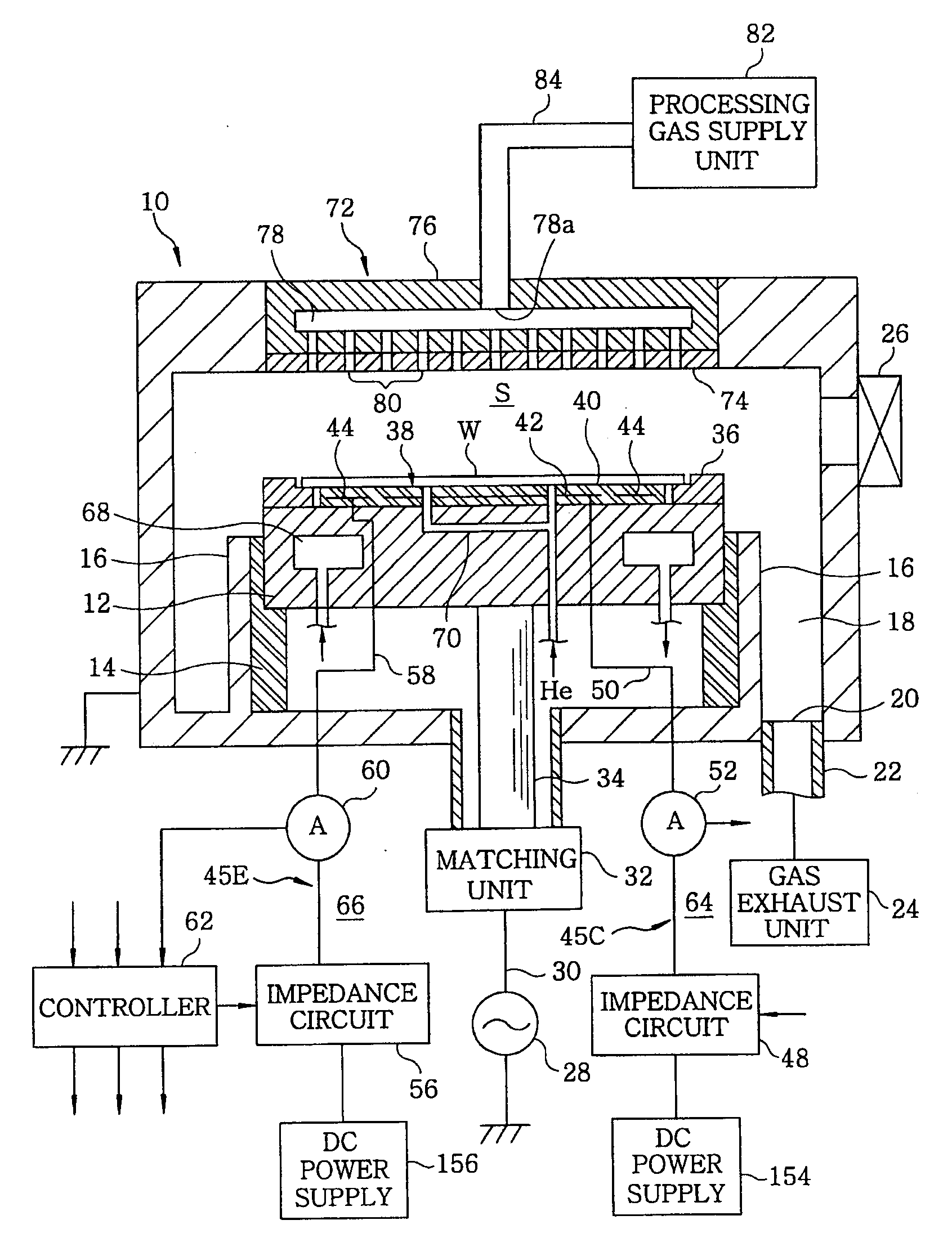
[0045]FIG. 1 illustrates a configuration of a plasma processing apparatus in accordance with the present invention. The plasma processing apparatus is configured as a capacitively coupled plasma etching apparatus of a cathode coupling type. The plasma processing apparatus comprises a cylindrical chamber (processing chamber) 10 made of metal such as aluminum or stainless steel. The chamber 10 is frame grounded.

[0046]A circular plate-shaped susceptor 12 serving as a lower electrode is horizontally disposed inside the chamber 10 to mount a target substrate, e.g., a semiconductor wafer W thereon. The susceptor 12 is made of, e.g., aluminum. The susceptor 12 is supported by an insulating cylindrical support portion 14 in a non-ground state, the cylindrical support portion 14 extending vertically upward from a bottom portion of the chamber 10 and made of, for example, ceramic. A conductive cylindrical supporting portion 16 extending upward from the bottom portion of the chamber 10 is form...

second embodiment

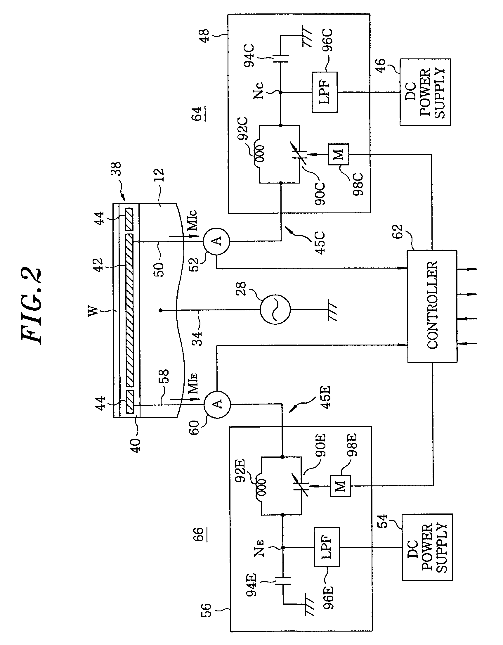
[0081]FIG. 6 illustrates exemplary configurations of the central and the peripheral impedance adjusting unit 164 and 166 in accordance with the

[0082]An impedance circuit 108 of the central impedance adjusting unit 164 includes the first and the second radio frequency LC circuit 112C and 114C, each having at least one variable reactance element. In the illustrated example, the first radio frequency LC circuit 112C is configured as an LC parallel circuit in which a variable capacitor 116C is connected in parallel to a coil 118C. The second radio frequency LC circuit 114C is configured as an LC parallel circuit in which a variable capacitor 120C is connected in parallel to a coil 122C. The DC voltage outputted from the DC power supply 46 flows through the LPF 96C, the coil 122C and the coil 118C and, then, is applied to the central conductor 42 of the electrostatic chuck 38 through the transmission line 50. The controller 62 may variably control the impedance positions of the variable ...

fourth embodiment

[0096]FIG. 9 illustrates a configuration of a plasma processing apparatus in accordance with the present invention. This plasma processing apparatus includes the electrostatic chuck 38 for attractively holding the wafer and a heating element 140 for heating the wafer on the wafer mounting portion of the upper surface of the susceptor 12. The electrostatic chuck 38 includes the film-shaped or plate-shaped dielectric member 40 which is integrally formed or fixed on the upper surface of the susceptor 12. The dielectric member 40 includes a mesh-shaped conductor 43 embedded therein, the conductor 43 being electrically connected to an external DC power supply 142 that is disposed at the outside of the chamber 10 via a switch 144, a high resistance resistor 146 and a DC high voltage line 148. Accordingly, the semiconductor wafer W can be attractively held on the electrostatic chuck 38 by a Coulomb force due to a high DC voltage applied from the DC power supply 142.

[0097]The heating elemen...


PUM

PropertyMeasurementUnit
Temperatureaaaaaaaaaa
Forceaaaaaaaaaa
Poweraaaaaaaaaa

Abstract

In a plasma processing apparatus comprising an evacuable processing chamber, a first electrode disposed in the processing chamber via an insulating body and a second electrode disposed in the processing chamber to face the first electrode, a central conductor and a peripheral conductor are embedded in a main surface of the first electrode via an insulating material while being separately disposed at an electrode central portion and an electrode peripheral portion, respectively. A first radio frequency leaking unit leaks a first radio frequency power applied to the first electrode from a first radio frequency power supply through at least one of the central conductor and the peripheral conductor by a desired current amount.

Description

FIELD OF THE INVENTION[0001]The present invention relates to a technology for performing a plasma process on a target substrate; and, more particularly, a capacitively coupled plasma processing apparatus which applies a radio frequency power to an electrode to generate a plasma.BACKGROUND OF THE INVENTION[0002]In a manufacturing process of a semiconductor device or flat panel display (FPD), a plasma is frequently used to obtain a good reaction of a processing gas at a relatively low temperature in an etching, deposition, oxidation, or sputtering process or the like. Conventionally, a capacitively coupled plasma processing apparatus capable of easily realizing a large-diameter plasma has been widely employed as a single-wafer plasma processing apparatus, especially, a plasma etching apparatus.[0003]Generally, in the capacitively coupled plasma processing apparatus, an upper electrode and a lower electrode are disposed to face each other in parallel in a vacuum processing chamber, and...

Claims


Application Information

Patent Timeline
IPC IPC(8): C23C16/505
CPCH01J37/32091H01J37/32183
Inventor YAMAZAWA, YOHEI
Owner TOKYO ELECTRON LTD
Why Eureka
Try Eureka