
Method to form a memory cell comprising a carbon nanotube fabric element and a steering element

a technology of carbon nanotube fabric and steering element, which is applied in the direction of digital storage, instruments, semiconductor devices, etc., can solve the problem and achieve the effect of reducing the difficulty of forming and maintaining such an empty spa

Inactive Publication Date: 2008-10-02
SANDISK TECH LLC
View PDF23 Cites 100 Cited by
  • Summary
  • Abstract
  • Description
  • Claims
  • Application Information

AI Technical Summary

Benefits of technology

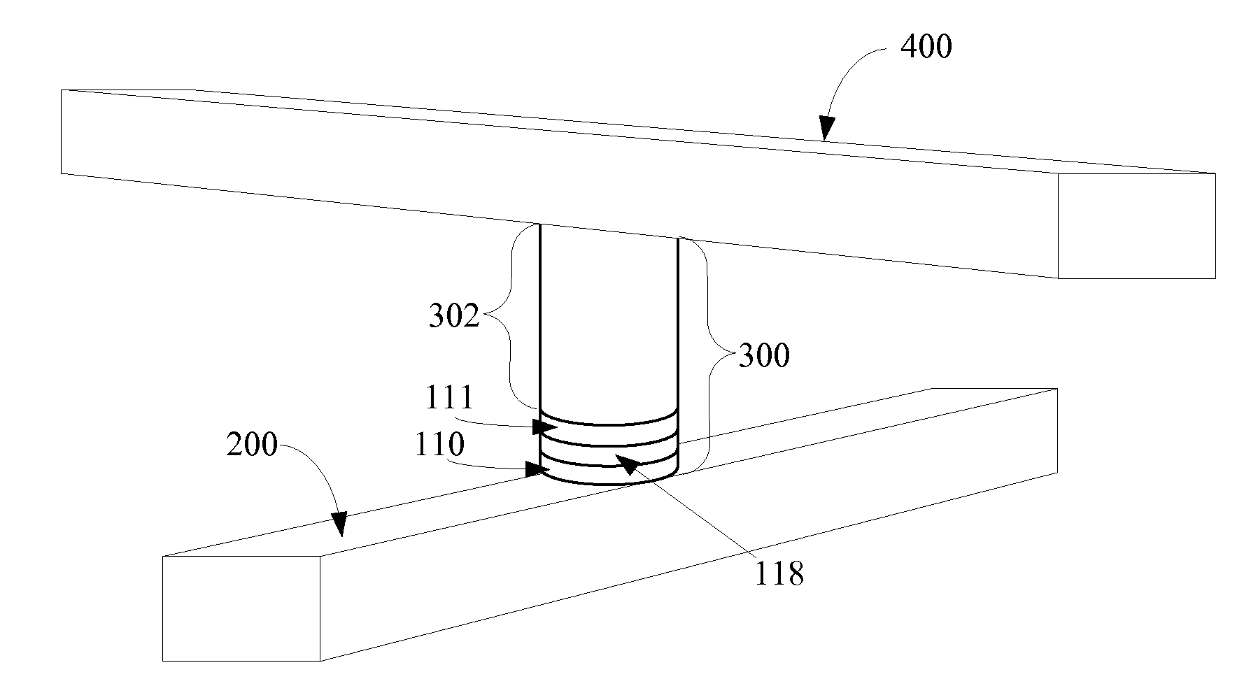
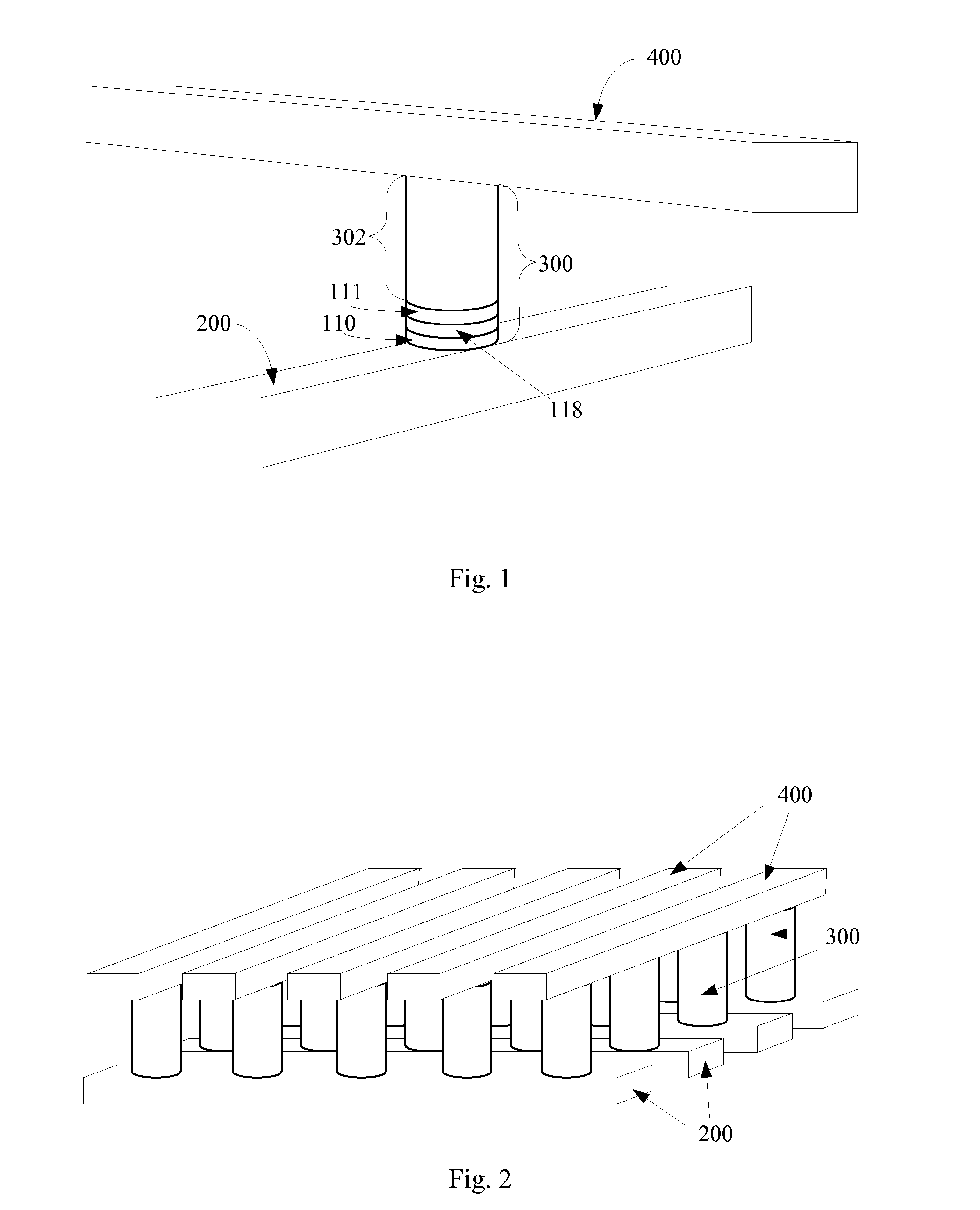
The present invention is about a method to create a memory array using carbon nanotube fabric and a steering element, such as a diode or transistor, arranged electrically in series. The method includes programming the carbon nanotube memory cell by applying a set pulse between the first and second conductors, which results in a decrease in resistivity of the carbon nanotube fabric. The technical effect of this invention is to provide a reliable and efficient method for programming carbon nanotube memory cells.

Problems solved by technology

In nanotechnologies, forming and maintaining such an empty space is extremely difficult.

Method used


Image

  • Method to form a memory cell comprising a carbon nanotube fabric element and a steering element
  • Method to form a memory cell comprising a carbon nanotube fabric element and a steering element
  • Method to form a memory cell comprising a carbon nanotube fabric element and a steering element

Examples


example

[0036]Turning to FIG. 5a, formation of the memory begins with a substrate 100. This substrate 100 can be any semiconducting substrate known in the art, such as monocrystalline silicon, IV-IV compounds like silicon-germanium or silicon-germanium-carbon, III-V compounds, II-VII compounds, epitaxial layers over such substrates, or any other semiconducting material. The substrate may include integrated circuits fabricated therein.

[0037]An insulating layer 102 is formed over substrate 100. The insulating layer 102 can be silicon oxide, silicon nitride, Si—C—O—H film, or any other suitable insulating material.

[0038]The first conductors 200 are formed over the substrate 100 and insulator 102. An adhesion layer 104 may be included between the insulating layer 102 and the conducting layer 106 to help conducting layer 106 adhere to insulating layer 102. If the overlying conducting layer 106 is tungsten, titanium nitride is preferred as adhesion layer 104. Conducting layer 106 can comprise any...


PUM


Abstract

A method to form a rewriteable nonvolatile memory cell is disclosed, the cell comprising a steering element in series with a carbon nanotube fabric. The steering element is preferably a diode, but may also be a transistor. The carbon nanotube fabric reversibly changes resistivity when subjected to an appropriate electrical pulse. The different resistivity states of the carbon nanotube fabric can be sensed, and can correspond to distinct data states of the memory cell. A first memory level of such memory cells can be monolithically formed above a substrate, a second memory level monolithically formed above the first, and so on, forming a highly dense monolithic three dimensional memory array of stacked memory levels.

Description

RELATED APPLICATIONS[0001]This application is related to Herner et al., U.S. patent application Ser. No. ______, (Atty. Docket No. SAND-01193US1), “Memory Cell Comprising a Carbon Nanotube Fabric Element and a Steering Element”; to Herner, U.S. patent application Ser. No. ______, (Atty. Docket No. SAND-01179US0), “Method to Form Upward-Pointing P-I-N Diodes Having Large and Uniform Current”; and to Herner, U.S. patent application Ser. No. ______, (Atty. Docket No. SAND-01179US1), “Large Array of Upward-Pointing P-I-N Diodes Having Large and Uniform Current,” all filed on even date herewith and all hereby incorporated by reference in their entirety.BACKGROUND OF THE INVENTION[0002]Carbon nanotube memories are believed to operate by flexing of individual carbon nanotubes or carbon nanotube ribbons in an electric field. This flexing mechanism requires space within which the carbon nanotubes can flex. In nanotechnologies, forming and maintaining such an empty space is extremely difficul...

Claims


Application Information

Patent Timeline
Patent Type & Authority Applications(United States)
IPC IPC(8): G11C11/36H10B99/00
CPCB82Y10/00G11C13/025G11C2213/71G11C2213/72G11C2213/79H01L27/24H01L27/285H01L51/0048H01L51/0595Y10S977/742H10B63/34H10B63/84H10B63/20H10B63/30H10B63/80H10N70/20H10N70/8845H10N70/826H10K85/221H10K10/701H10K19/202
Inventor HERNER, S. BRADSCHEUERLEIN, ROY E.
Owner SANDISK TECH LLC
Learn More