Ag-based alloy wire for semiconductor package

a technology of alloy wires and semiconductors, applied in the field of silver alloy wires for wire bonding, can solve the problems of reducing bonding strength, limiting cost reduction, and reliability problems of ag wires, and achieve the effect of low manufacturing cost and high reliability

Inactive Publication Date: 2008-10-02
MK ELECTRON
View PDF7 Cites 50 Cited by
  • Summary
  • Abstract
  • Description
  • Claims
  • Application Information

AI Technical Summary

Benefits of technology

[0009]The present invention provides an Ag-based alloy wire for a semicond

Problems solved by technology

However, such Au—Ag alloy wires still include Au at high composite rates, which limits the cost reduction.
However, the Ag wire has a reliability problem when bonded to the aluminum (Al) pad.
Particularly as illustrated in FIG. 1, when performing a high humidity reliability test, a bonding surface of the Ag wire and th

Method used


Image

  • Ag-based alloy wire for semiconductor package

Examples


Embodiment Construction

[0016]The present invention will now be described more fully with reference to the accompanying drawings, in which exemplary embodiments of the invention are shown. The invention may, however, be embodied in many different forms and should not be construed as being limited to the embodiments set forth herein; rather, these embodiments are provided so that this disclosure will be thorough and complete, and will fully convey the concept of the invention to those skilled in the art.

[0017]A wire for a semiconductor package according to embodiments of the present invention is used for bonding a semiconductor chip to a package substrate. Thus, the wire for the semiconductor package according to embodiments of the present invention may be referred to as a bonding wire.

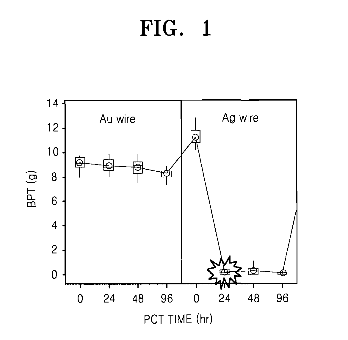
[0018]An Ag-based alloy wire according to embodiments of the present invention may be formed by alloying a predetermined quantity of additive ingredients into pure Ag. However, although not specially mentioned, the Ag-based a...


PUM


Abstract

An Ag-based alloy wire for a semiconductor package is highly reliable and can be fabricated with low costs. The Ag-based alloy wire includes 0.05˜5 wt % of at least one kind of a first additive ingredient selected from the group consisting of platinum (Pt), palladium (Pd), rhodium (Rh), osmium (Os), gold (Au), and nickel (Ni), and Ag as a remainder.

Description

CROSS-REFERENCE TO RELATED PATENT APPLICATION[0001]This application claims the benefit of Korean Patent Application No. 10-2007-0031998, filed on Mar. 30, 2007, in the Korean Intellectual Property Office, the disclosure of which is incorporated herein in its entirety by reference.BACKGROUND OF THE INVENTION[0002]1. Field of the Invention[0003]The present invention relates to a semiconductor package, and more particularly to a silver (Ag)-based alloy wire for wire bonding.[0004]2. Description of the Related Art[0005]In semiconductor packages, semiconductor chips can be electrically connected to a package substrate using wire bonding. In conventional semiconductor packages, an aluminum pad of a semiconductor chip and a package substrate are bonded using gold (Au) wires. Au has been widely used because of its high chemical stability and high electrical conductivity. However, in order to meet the continuous demand to decrease the manufacturing costs in the semiconductor industry and add...

Claims


Application Information

Patent Timeline
IPC IPC(8): C22C5/06C22C5/08
CPCC22C5/06H01L2224/05624C22C5/08H01L2224/45144H01L24/45H01L2224/45139H01L2924/01047H01L2224/48624H01L2924/00H01L2924/01078H01L2924/01046H01L2924/01045H01L2924/01076H01L2924/01079H01L2924/01028H01L2924/01029H01L2924/01004H01L2924/0102H01L2924/01012H01L2924/01056H01L2924/01057H01L2924/01058H01L2924/01039H01L2924/00015H01L2224/45015H01L2224/43848H01L24/43H01L2924/00011H01L2924/013H01L2924/00014H01L2924/01048H01L2924/01014H01L2924/01022H01L2924/00013H01L2924/01049H01L2924/20753H01L21/30
Inventor CHO, JONG SOOMOON, JEONG TAK
Owner MK ELECTRON
Why Eureka
Try Eureka