Method for forming strained silicon nitride films and a device containing such films

a technology of silicon nitride and strained films, which is applied in the field of semiconductor processing, can solve the problems of reducing throughput, requiring expensive special purpose tooling, and limiting the control of strain amoun

Active Publication Date: 2008-10-02
TOKYO ELECTRON LTD
View PDF9 Cites 511 Cited by
  • Summary
  • Abstract
  • Description
  • Claims
  • Application Information

AI Technical Summary

Benefits of technology

[0007]Thus, one aspect of the invention is to reduce or eliminate one or more o...

Problems solved by technology

First, post processing of the deposited film increases production steps thereby reducing throughput, and may require expensive special purpose tooling.
In addition, post processing of the deposited film primarily affects the film surface, which limits control of the ...

Method used


Image

  • Method for forming strained silicon nitride films and a device containing such films
  • Method for forming strained silicon nitride films and a device containing such films
  • Method for forming strained silicon nitride films and a device containing such films

Examples


Embodiment Construction

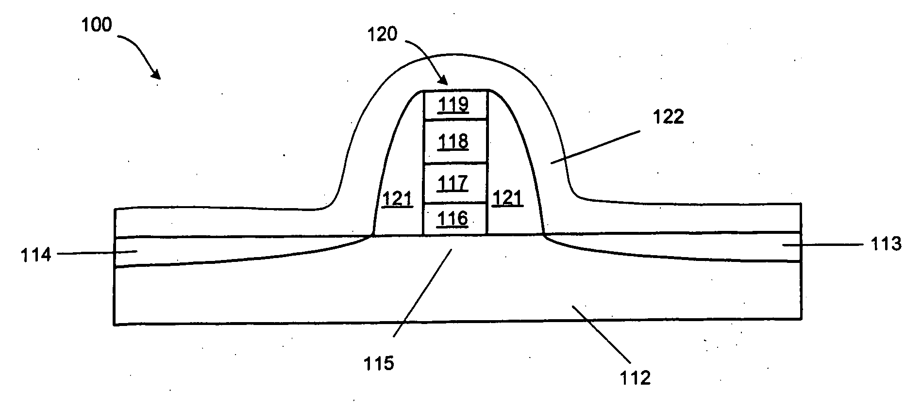
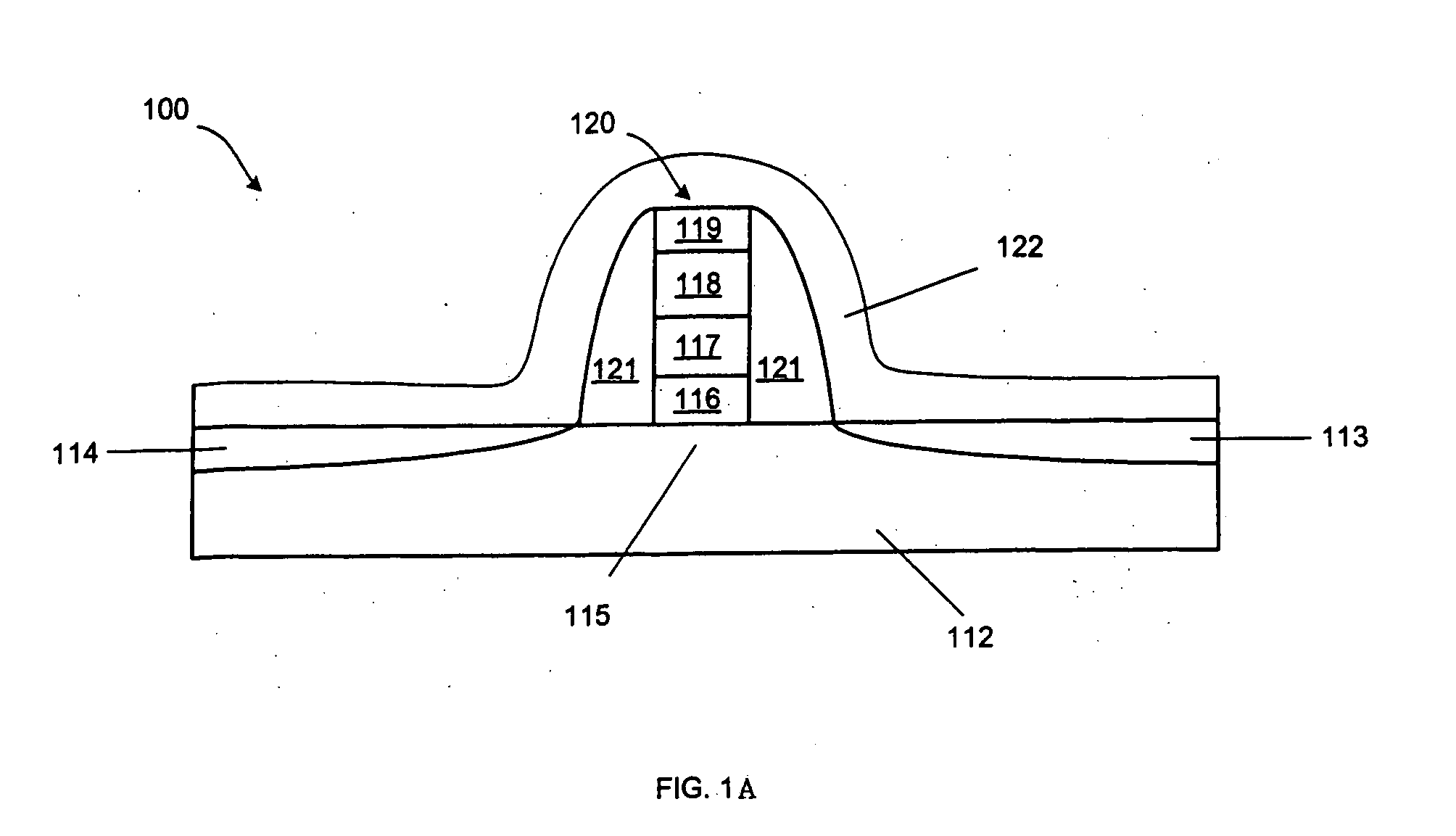
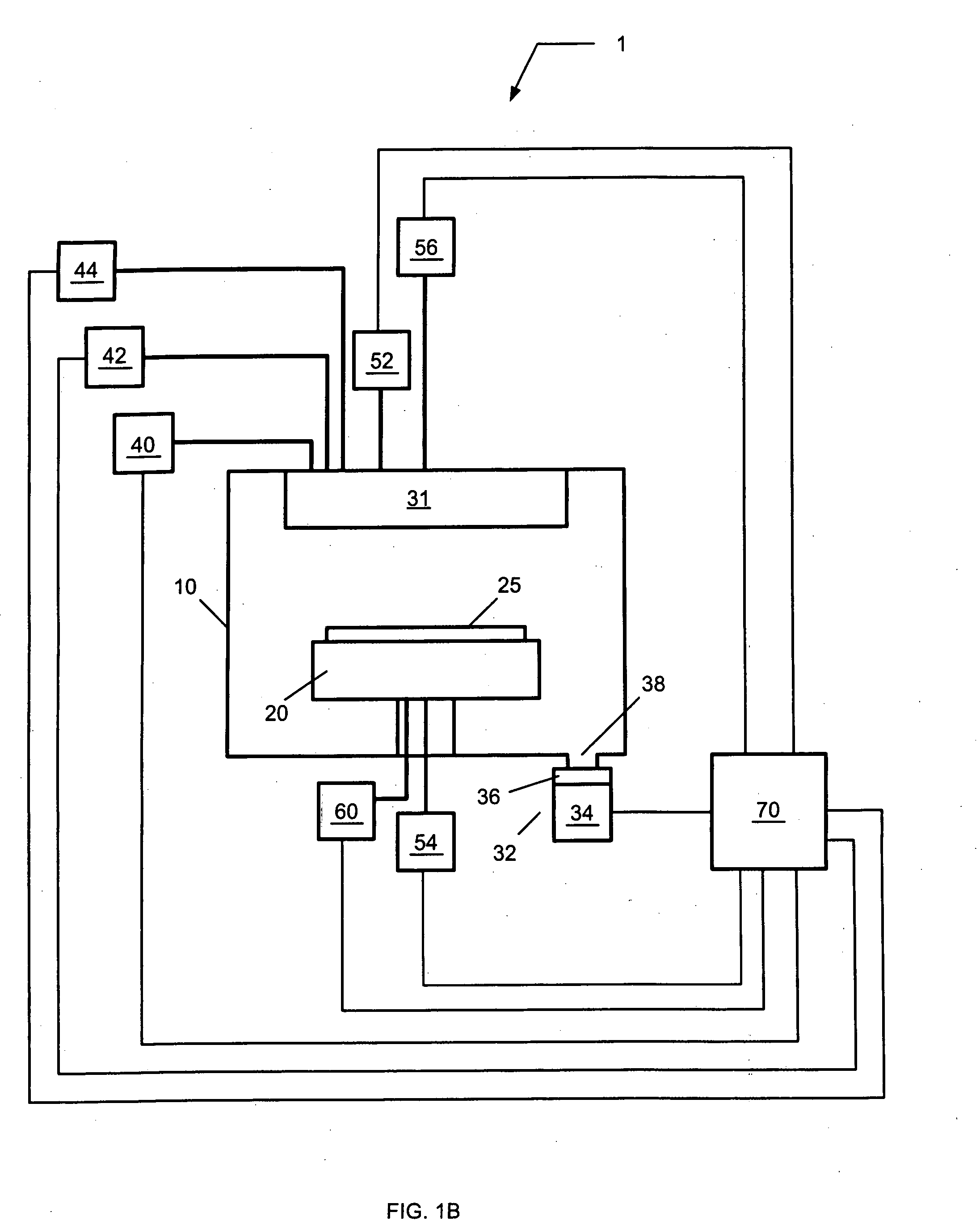
[0016]Embodiments of the invention describe processing methods to deposit strained SiN films in a process chamber. According to embodiments of the invention, a difference in reactivity of a nitrogen precursor towards a,silicon precursor is utilized to deposit SiN films having a density gradient across the film thickness. A difference in reactivity is achieved by varying plasma activation of the nitrogen precursor during processing. For example, the reactivity may be controlled by the type of plasma activation and the level of plasma power used for the activation. According to embodiments of the invention, plasma activation may be accomplished using a direct plasma source within the process chamber or using a remote plasma source.

[0017]For example, the plasma activation may be utilized to vary the SiN deposition rate and film density. In some cases this difference in density may be further affected by changing the silicon precursor, changing the nitrogen precursor and / or changing oth...


PUM

PropertyMeasurementUnit
Ratioaaaaaaaaaa
Plasma poweraaaaaaaaaa

Abstract

A method for forming a strained SiN film and a semiconductor device containing the strained SiN film. The method includes exposing the substrate to a gas including a silicon precursor, exposing the substrate to a gas containing a nitrogen precursor activated by a plasma source at a first level of plasma power and configured to react with the silicon precursor with a first reactivity characteristic, and exposing the substrate to a gas containing the nitrogen precursor activated by the plasma source at a second level of plasma power different from the first level and configured to react with the silicon precursor with a second reactivity characteristic such that a property of the silicon nitride film formed on the substrate changes to provide the strained silicon nitride film.

Description

CROSS-REFERENCE TO RELATED APPLICATIONS[0001]This application is related to co-pending U.S. patent application Ser. No. 11 / XXX,XXX (Attorney Docket No. 304031US), entitled “STRAINED METAL NITRIDE FILMS AND METHOD OF FORMING,” filed on even date herewith; co-pending U.S. patent application Ser. No. 11 / XXX,XXX (Attorney Docket No. 306464US), entitled “STRAINED METAL NITRIDE FILMS AND METHOD OF FORMING,” filed on even date herewith; co-pending U.S. patent application Ser. No. 11 / XXX,XXX (Attorney Docket No. 306467US), entitled “STRAINED METAL SILICON NITRIDE FILMS AND METHOD OF FORMING,” filed on even date herewith; co-pending U.S. patent application Ser. No. 11 / XXX,XXX (Attorney Docket No. 306468US), entitled “STRAINED METAL SILICON NITRIDE FILMS AND METHOD OF FORMING,” filed on even date herewith, and co-pending U.S. patent application Ser. No. 11 / 529,380 (Attorney Docket No. 296626US), entitled “A METHOD OF FORMING STRAINED SILICON NITRIDE FILMS AND A DEVICE CONTAINING SUCH FILMS,” ...

Claims


Application Information

Patent Timeline
IPC IPC(8): H01L21/31
CPCC23C16/345C23C16/45542H01L29/7843H01L21/3185H01L29/78C23C16/515H01L21/02274H01L21/0228H01L21/02211H01L21/0217H01L21/31
Inventor CLARK, ROBERT D.
Owner TOKYO ELECTRON LTD
Why Eureka
Try Eureka