Methods for forming dense dielectric layer over porous dielectrics

Inactive Publication Date: 2008-10-02
ALSEPHINA INNOVATIONS INC
View PDF12 Cites 17 Cited by
  • Summary
  • Abstract
  • Description
  • Claims
  • Application Information

AI Technical Summary

Benefits of technology

[0010]A second aspect of the disclosure provides a method comprising: forming an opening in a inter-layer dielectric (ILD) on a wafer, the ILD having an ultra-low dielectric constant, wherein the opening has a sidewall surface and a bottom surface; and exposing the sidewall surface and the bottom surface to a plurality of substantially parallel ultra-violet (UV) radiation rays to form a dense dielectric layer having a substantially uniform thickness over both the sidewall surface and the bottom surface, and wherein the exposing comprises: exposing the bottom surface to the plurality of substantially parallel UV radiation rays at a first angle of incidence; and exposing the sidewall surface to the plurality of substantially parallel UV radiation rays at a second angle of incidence different than the first angle of incidence, the exposure to the bottom surface and the sidewall surface being substantially uniform.
[0011]A third aspect of the disclosure provides a method comprising: forming an opening in an inter-layer dielectric (ILD) on a wafer, the ILD having an ultra-low d

Problems solved by technology

This penetration or intrusion of metal into porous ULK ILDs may cause performance degradation of the metal interconnects formed thereon, as well as degradation of the insulating capability of the ILD.
In a worst case, this insulating degradation causes shorting between neighboring elements of the interconnect structure.
The interconnected porosity poses a challenge for the application of advanced liner processes (e.g., thermal and ion-induced atomic layer deposition (iALD), or plasma-enhanced chemical vapor deposition (PECVD)) due to chemical precursors penetrating in

Method used


Image

  • Methods for forming dense dielectric layer over porous dielectrics
  • Methods for forming dense dielectric layer over porous dielectrics
  • Methods for forming dense dielectric layer over porous dielectrics

Examples


Embodiment Construction

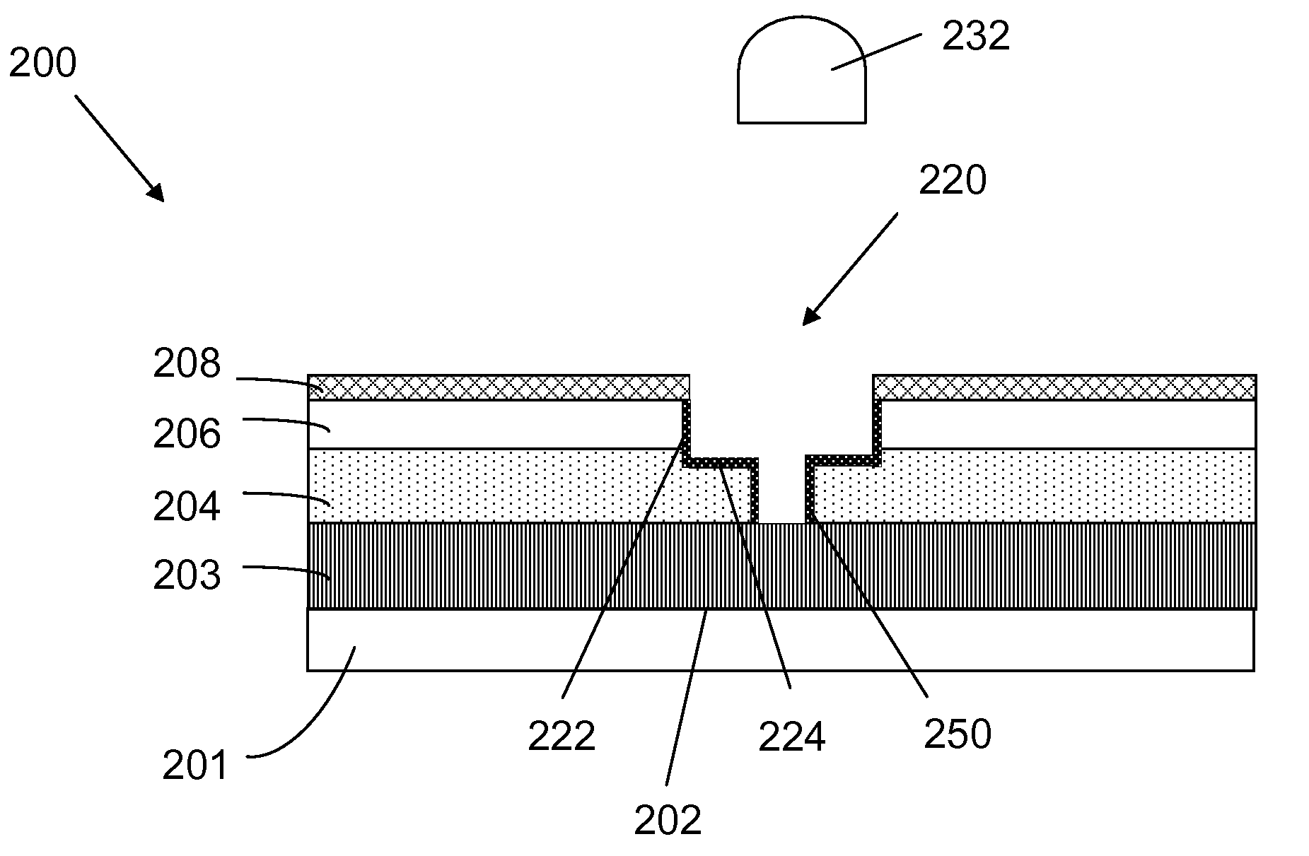
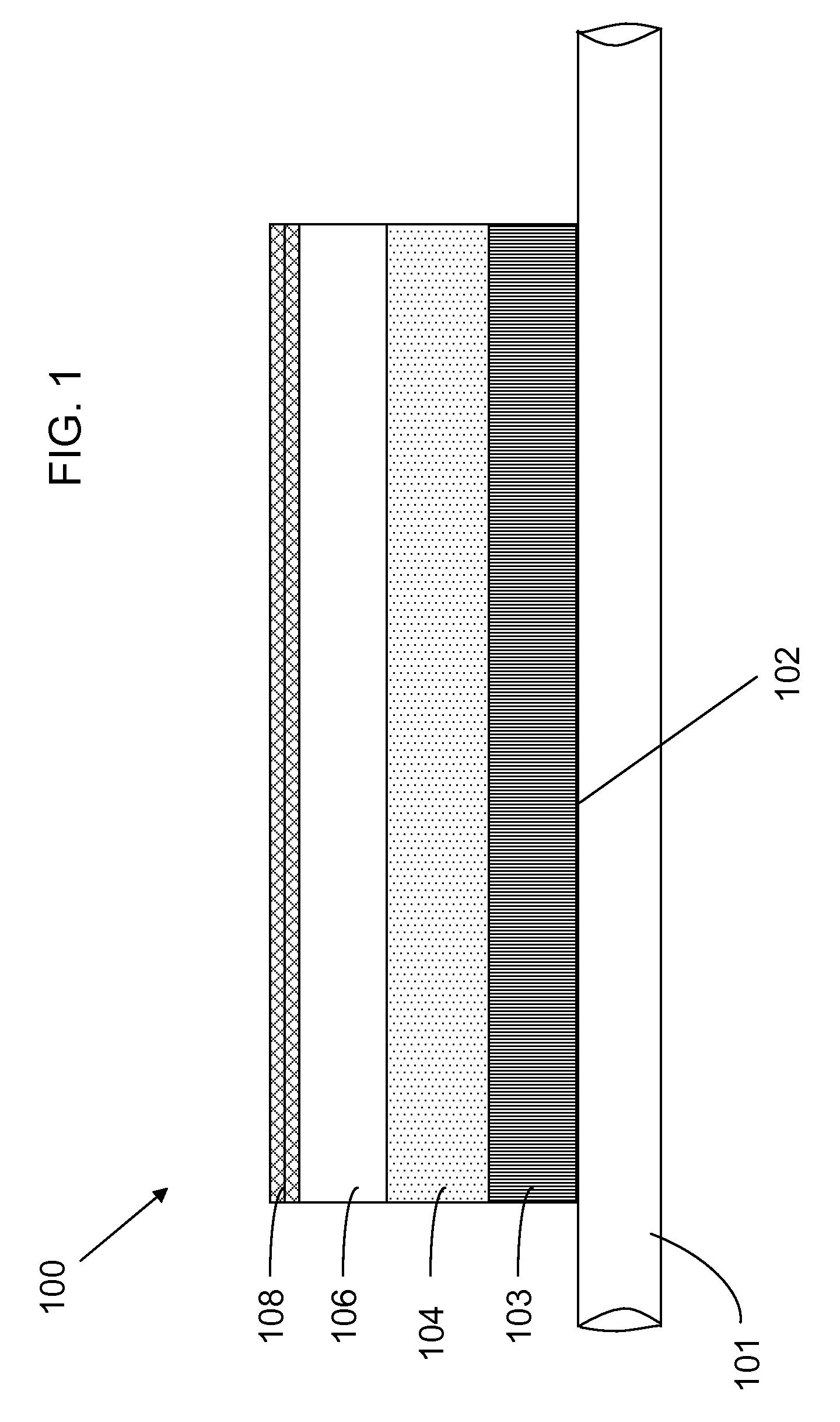
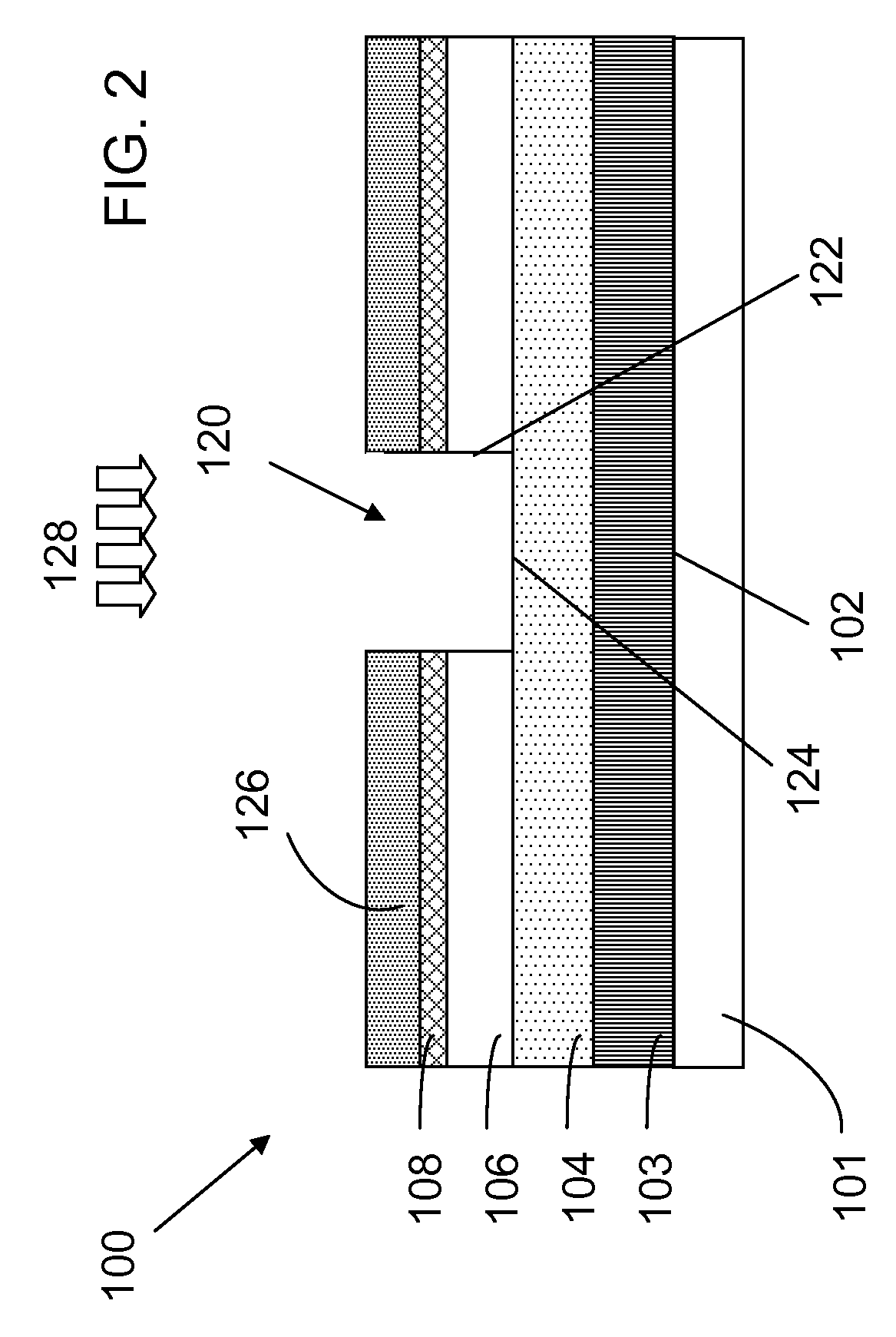
[0018]Turning to the drawings, FIG. 1 shows a preliminary structure 100 on a wafer 101, to which a method according to embodiments of the disclosure will be applied. Although a single structure 100 is shown for the sake of clarity, it should be appreciated that wafer 101 may include multiple structures. In this embodiment, an interconnect wiring network (not shown) is formed using a dual damascene (DD) process. In the DD process, an inter-metal dielectric (IMD or ILD), shown as two layers 104, 106, is coated on a substrate 103. Layer 104 (e.g., a via level dielectric) and layer 106 (e.g., a line level dielectric) are shown separately for clarity of the process flow description. Layers 104, 106 may be made of the same or different dielectric materials, and in the former case, applied as a single monolithic layer. A hard mask layer or a layered stack 108 is optionally employed to facilitate etch selectivity and to serve as a polish stop. Layers 104, 106 may be porous ultra low dielect...


PUM


Abstract

Methods for forming a dense dielectric layer over the surface of an opening in a porous inter-layer dielectric having an ultra-low dielectric constant are disclosed. The disclosure provides methods for exposing the sidewall surface and the bottom surface of the opening to a plurality of substantially parallel ultra-violet (UV) radiation rays to form a dense dielectric layer having a substantially uniform thickness over both the sidewall surface and the bottom surface.

Description

BACKGROUND OF THE DISCLOSURE[0001]1. Technical Field[0002]The disclosure relates generally to semiconductor fabrication, and more particularly, to forming a dense dielectric layer over the surface of an opening in a porous inter-layer dielectric having an ultra-low dielectric constant.[0003]2. Background Art[0004]Recent rapid advancement in semiconductor technology has brought the advent of very large scale integrated (VLSI) as well as ultra large scale integrated (ULSI) circuits, resulting in integration of more devices into smaller areas on a single semiconductor substrate. In order to further enhance performance of the VLSI and / or ULSI circuits, ultra-low dielectric constant (ULK) materials, such as porous materials, are being used as inter-level dielectrics (i.e., via level dielectrics) and intra-level dielectrics (i.e., line level dielectrics), both referred to as ILDs, herein. ILDs, alternatively known as inter-metal dielectrics (IMDs), are used to further reduce capacitance s...

Claims


Application Information

Patent Timeline
IPC IPC(8): H01L21/00
CPCH01L21/3105H01L21/31058H01L21/76808H01L21/76814H01L21/76825H01L21/76831H01L21/76835
Inventor DIMITRAKOPOULOS, CHRISTOS D.CHACE, MARK S.
Owner ALSEPHINA INNOVATIONS INC
Why Eureka
Try Eureka