Wafer polish monitoring method and device

a monitoring method and polish technology, applied in the direction of semiconductor/solid-state device testing/measurement, manufacturing tools, lapping machines, etc., can solve the problems of poor signal-to-noise ratio, difficult to detect the end point of each polishing process with precision, reflected light scattering, etc., to achieve easy detection of the characteristic impedance of the microstrip line, easy to form, and easy to bury

Inactive Publication Date: 2008-10-02
TOKYO SEIMITSU
View PDF2 Cites 13 Cited by
  • Summary
  • Abstract
  • Description
  • Claims
  • Application Information

AI Technical Summary

Benefits of technology

[0077]The seventeenth aspect of the invention is a wafer polish monitoring device in which the microstrip line is formed with a strip conductor that is supported on a ground plane via a dielectric material, and the strip conductor lies parallel to the ground plane. This wafer polish monitoring device has the advantage that the microstrip line can be readily formed and can be made small, and the small-sized microstrip line can be easily buried in the upper face portion of the platen.
[0078]The eighteenth aspect of the invention is a wafer polish monitoring device in which the dielectric material in the microstrip line is Teflon (a registered trade name), epoxy, or Bakelite. This wafer polish monitoring device has the advantage that the characteristic impedance of the microstrip line can be easily determined, and the high-frequency loss can be restricted to a small amount.
[0079]The nineteenth aspect of the invention is a wafer polish monitoring device in which the high-frequency transmission path is formed with a cavity resonator. In this wafer polish monitoring device, the transmission coefficient, the reflection coefficient, and the loss coefficient can be greatly varied with the change in the film thickness after the polishing of the conductive film progresses and the film thickness of the conductive film decreases to the extremely small film thickness defined by the skin depth. Accordingly, this wafer polish monitoring device has the advantage that the end point of the polishing removal of the conductive film can be detected with high precision and accuracy, based on the variations of those coefficients.
[0080]The twentieth aspect of the invention is a wafer polish monitoring device in which the cavity resonator is capable of changing the resonant frequency by changing the volume or shape of the cavity portion. This wafer polish monitoring device has the advantage that the resonant frequency of the cavity resonator can be arbitrarily adjusted, and accordingly, the transmission coefficient, the reflection coefficient, and the loss coefficient can be greatly varied with the change in the film thickness after the polishing of the conductive film progresses and the film thickness of the conductive film decreases to the extremely small film thickness defined by the skin depth.
[0081]The twenty-first aspect of the invention is a wafer polish monitoring device in which the upper face of the cavity resonator is covered with a nonconductor material. This wafer polish monitoring device has the advantage that, only when there is a wafer having a conductive film formed thereon, the film condition of the conductive film is monitored with precision, and the variations of the required coefficients such as the transmission coefficient and the reflection coefficient of the electromagnetic waves can be obtained.
[0082]The twenty-second aspect of the invention is a wafer polish monitoring device in which the high-frequency transmission path is formed between a transmission antenna connected to a transmitter and a reception antenna connected to a receiver. In this wafer polish monitoring device, the variations of the coefficients such as the transmission coefficient and the reflection coefficient of the electromagnetic waves are caused by the characteristic impedance of the high-frequency transmission path varying with the change in the film thickness, after the polishing of the conductive film progresses and the film thickness of the conductive film decreases to the extremely small film thickness defined by the skin depth. Accordingly, this wafer polish monitoring device has the advantage that the end point of the polishing removal of the conductive film can be detected with precision, based on the variations of those coefficients.

Problems solved by technology

However, this method has the problem of reflected light scattering due to the slurry.
As a result, the signal-to-noise ratio is poor, and it is difficult to detect the end point of each polishing process with precision.
Furthermore, there is not a clear definition of “reflection of microwaves”.

Method used


Image

  • Wafer polish monitoring method and device
  • Wafer polish monitoring method and device
  • Wafer polish monitoring method and device

Examples


first embodiment

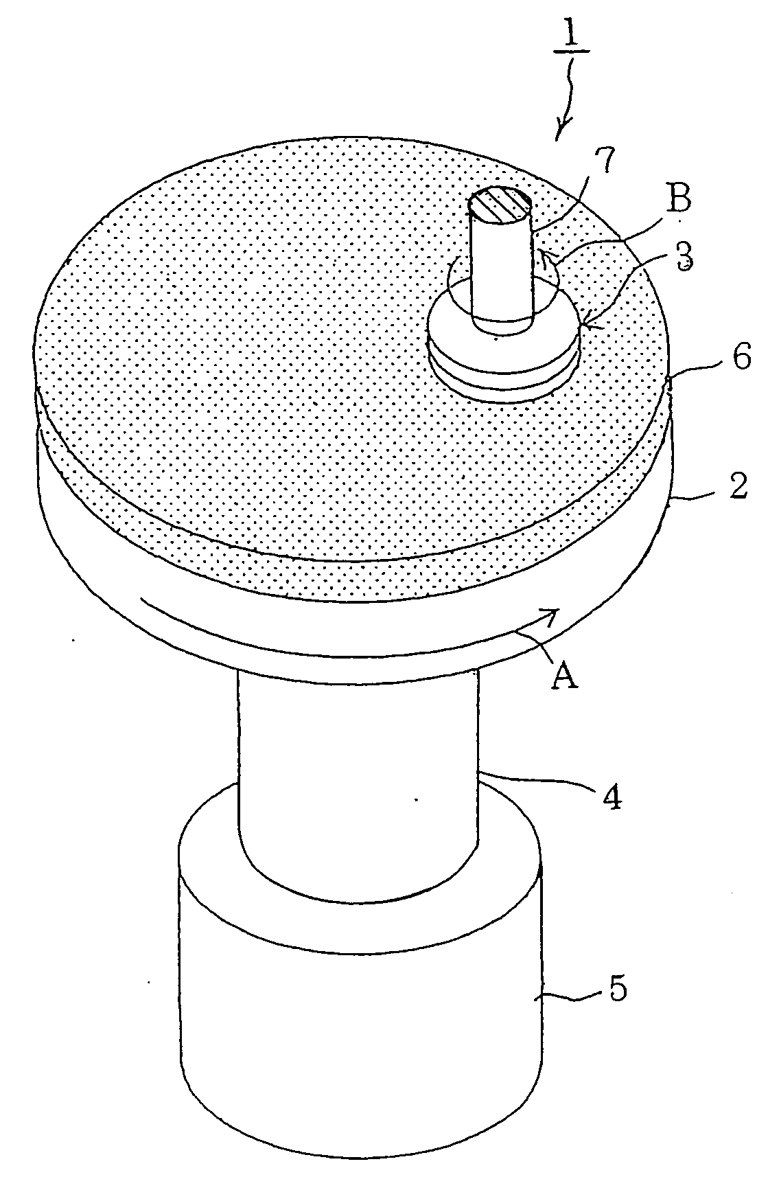
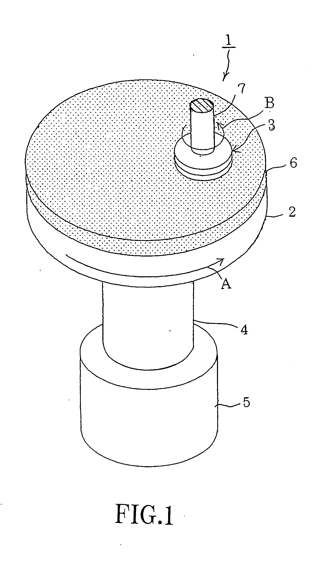
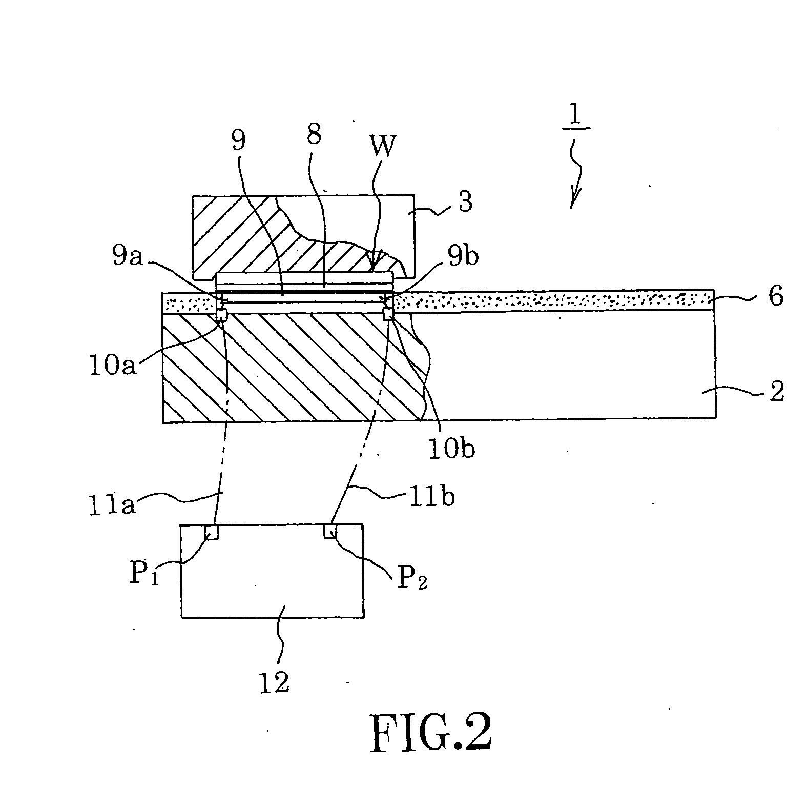
[0096]The following is a description of a preferred embodiment of the present invention, with reference to the accompanying drawings. FIG. 1 is a perspective view of a chemical mechanical polishing device equipped with a microstrip line. FIG. 2 is a configuration diagram illustrates the connection between the microstrip line mounted on the upper face portion of the platen and a network analyzer.

[0097]First, the wafer polish monitoring method and a configuration of the device in accordance with this embodiment are described, with a chemical mechanical polishing device as a processing device being taken as an example. In FIG. 1, a chemical mechanical polishing device 1 mainly includes a platen 2 and a polishing head 3.

[0098]The platen 2 is formed in a disk-like form. A rotation axis 4 is connected to the center of the bottom face of the platen 2, and the platen 2 rotates in the direction indicated by an arrow A when a motor 5 is driven. A polishing pad 6 is bonded onto the upper face ...


PUM

PropertyMeasurementUnit
resistanceaaaaaaaaaa
frequencyaaaaaaaaaa
frequencyaaaaaaaaaa

Abstract

The present invention aims to provide a wafer polish monitoring method and device for detecting the end point of the polishing of a conductive film with high precision and accuracy by monitoring the variation of the film thickness of the conductive film without adverse influence of slurry or the like after the film thickness of the conductive film decreases to an extremely small film thickness defined by the skin depth. To achieve this objective, the present invention provides a wafer polish monitoring method by which a high-frequency transmission path is formed in a portion facing the conductive film on the surface of the wafer, the polishing removal state of the conductive film is evaluated based at least on the transmitted electromagnetic waves passing through the high-frequency transmission path or the reflected electromagnetic waves that are reflected without passing through the high-frequency transmission path, and the end point of the polishing removal and the point equivalent to the end point of the polishing removal are detected.

Description

BACKGROUND OF THE INVENTION[0001]1. Field of the Invention[0002]The present invention relates to a wafer polish monitoring method and device, and more particularly, to a wafer polish monitoring method and device that can detect, with high precision, the end point of the polishing of the conductive film formed on a wafer in a chemical mechanical polishing (CMP) process, or the like.[0003]2. Description of the Related Art[0004]An oxide film, for example, is formed on the surface of a semiconductor wafer, and a groove pattern equivalent to a wiring pattern is formed by processing the oxide film by lithography or an etching technique. A conductive film made of Cu or the like is formed thereon to fill the groove pattern. The unnecessary portion of the conductive film is then removed by CMP, so as to form the wiring pattern. This process is a well known process. In the formation of the wiring pattern or the like, it is critical to detect the end point of the polishing with precision and s...

Claims


Application Information

Patent Timeline
Patent Type & Authority Applications(United States)
IPC IPC(8): B24B49/00B24B37/013H01L21/304
CPCB24B49/10H01L22/26H01L21/304
Inventor FUJITA, TAKASHIYOKOYAMA, TOSHIYUKIKITADE, KEITA
Owner TOKYO SEIMITSU
Why Eureka
Try Eureka