

Storage device equipped with NAND flash memory and method for storing information thereof
a storage device and flash memory technology, applied in the direction of memory architecture accessing/allocation, instruments, computing, etc., can solve the problems of lower silicon efficiency, inability to fully take the advantages of flash memory such as fast read/write speed, less power consumption, and large size of solid-state hard disks made from slc flash memory, etc., to achieve fast information access speed, enhance processing performance, and increase the data density of each storage unit
- Summary
- Abstract
- Description
- Claims
- Application Information
AI Technical Summary
Benefits of technology
Problems solved by technology
Method used
Image

Examples
first embodiment
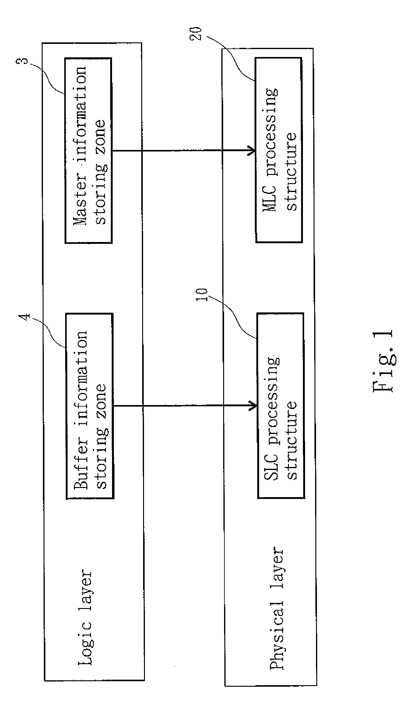
[0019]Please refer to FIG. 1 for the structure of the invention. The storage device equipped with NAND flash memory of the invention includes:
[0020]a SLC processing structure 10 to store one bit of information by applying a voltage on electric charges of a floating gate of a first transistor (not shown in the drawing) which has a first source to remove the electric charges to erase the one bit information; and
[0021]a MLC processing structure 20 to store two bits of information by applying a voltage on a plurality of electric charges of differential potentials on a floating gate of a second transistor which has a second source to erase the two bits of information by removing the stored electric charges. The physical and circuit structures of NAND logic flash memory, SLC processing structure 10 and MLC processing structure 20 are known in the art and form no part of the invention, thus details are omitted.
[0022]By means of the construction set forth above, the SLC processing structure...
third embodiment
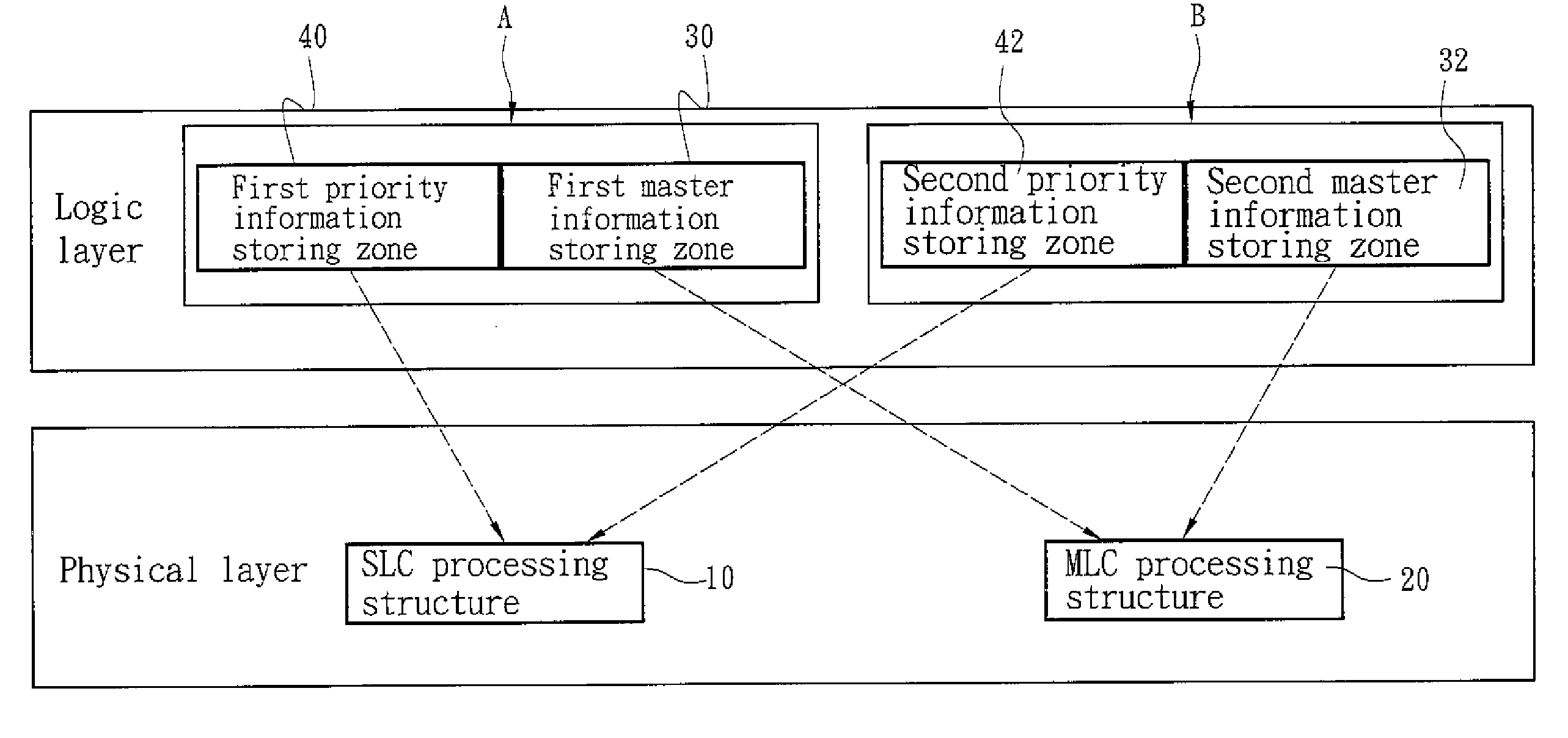
[0026]Refer to FIG. 3 for flowchart-1 of the invention that is an information storing method adopted for use on the storage device equipped with NAND logic flash memory previously discussed. The method includes the steps of:
[0027]getting an information (S1);
[0028]setting a priority of the information according to a priority authorization (S2);
[0029]determining a sequence for storing the information in the SLC processing structure 10 or the MLC processing structure 20 according to the priority; and
[0030]getting a remained storage space condition of the SLC processing structure 10 and the MLC processing structure 20 (S3), and determining whether to store the information to either the SLC processing structure 10 or the MLC processing structure 20 according to the priority of the information (S4).
[0031]For instance, in the event that the priority authorization setting sets a higher priority for the SLC processing structure 10 to store information of a higher priority (such as operating ...
PUM
 Abstract
Description
Claims
Application Information