

Semiconductor-encapsulating resin composition and semiconductor device
a technology of semiconductor devices and resin compositions, which is applied in the direction of semiconductor/solid-state device details, non-metal conductors, conductors, etc., can solve the problems of semiconductor devices being detachable, semiconductor devices receiving explosive stress due to vaporized steam, and cracks in semiconductor devices
- Summary
- Abstract
- Description
- Claims
- Application Information
AI Technical Summary
Benefits of technology
Problems solved by technology
Method used
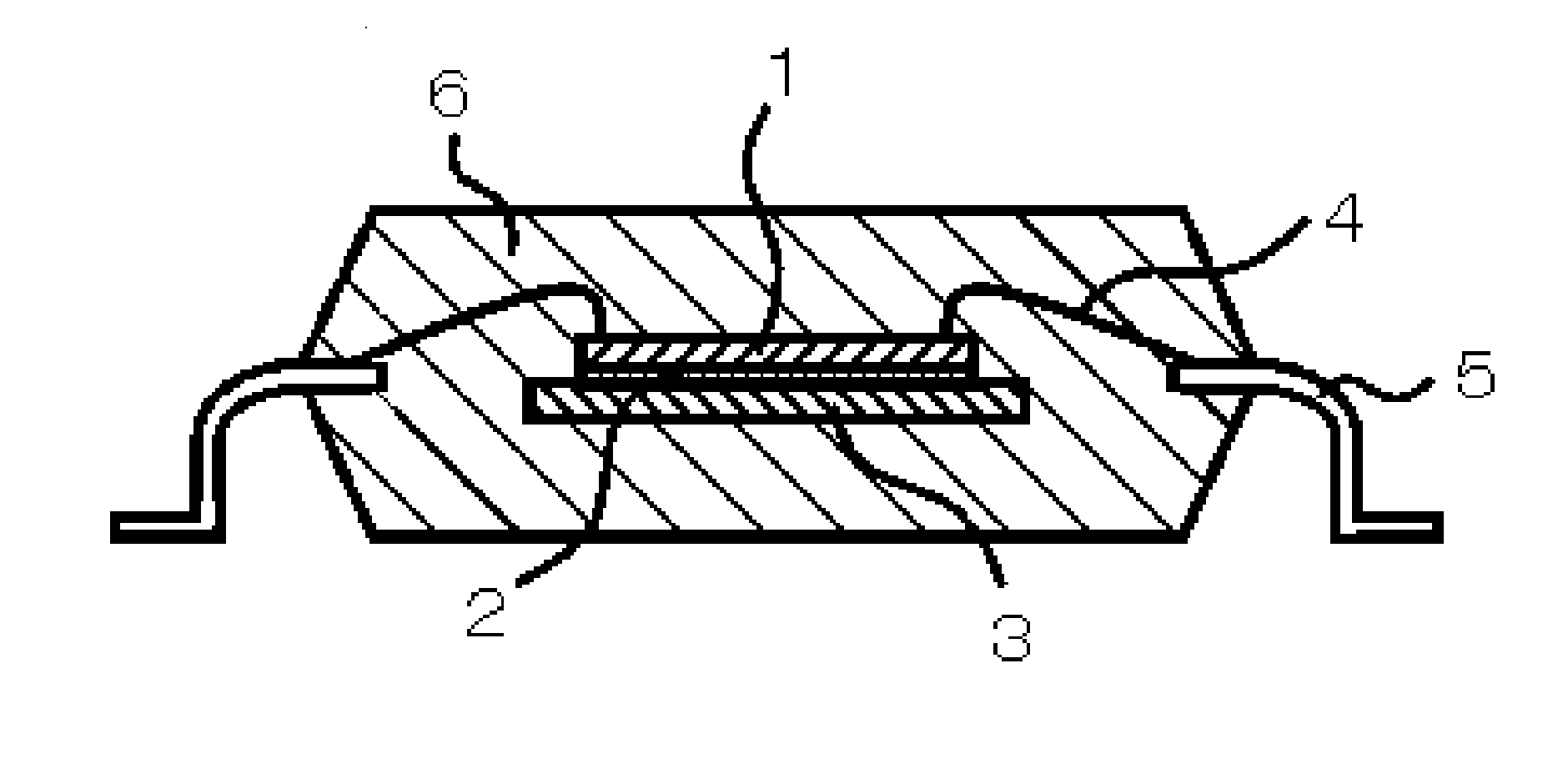
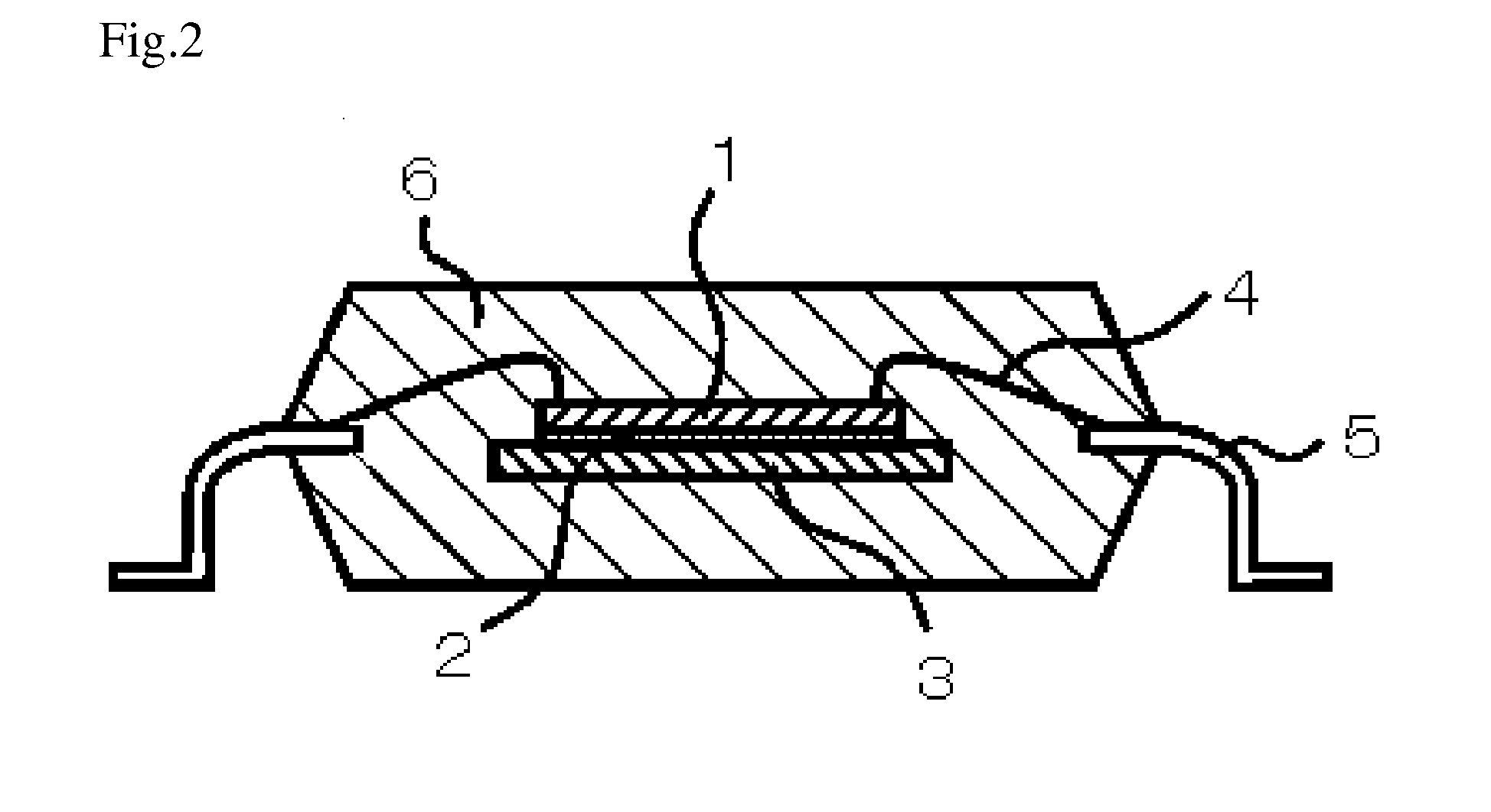
Image

Examples
example 1
[0135]
[0136]The above components were mixed with a mixer at room temperature. The mixture was melt-kneaded with a heating roller at 80° C. or higher and 100° C. or lower, cooled, and then crushed. Thus, an epoxy resin composition was obtained. The prepared epoxy resin composition was evaluated by the following methods. The evaluation results are shown in Table 2.
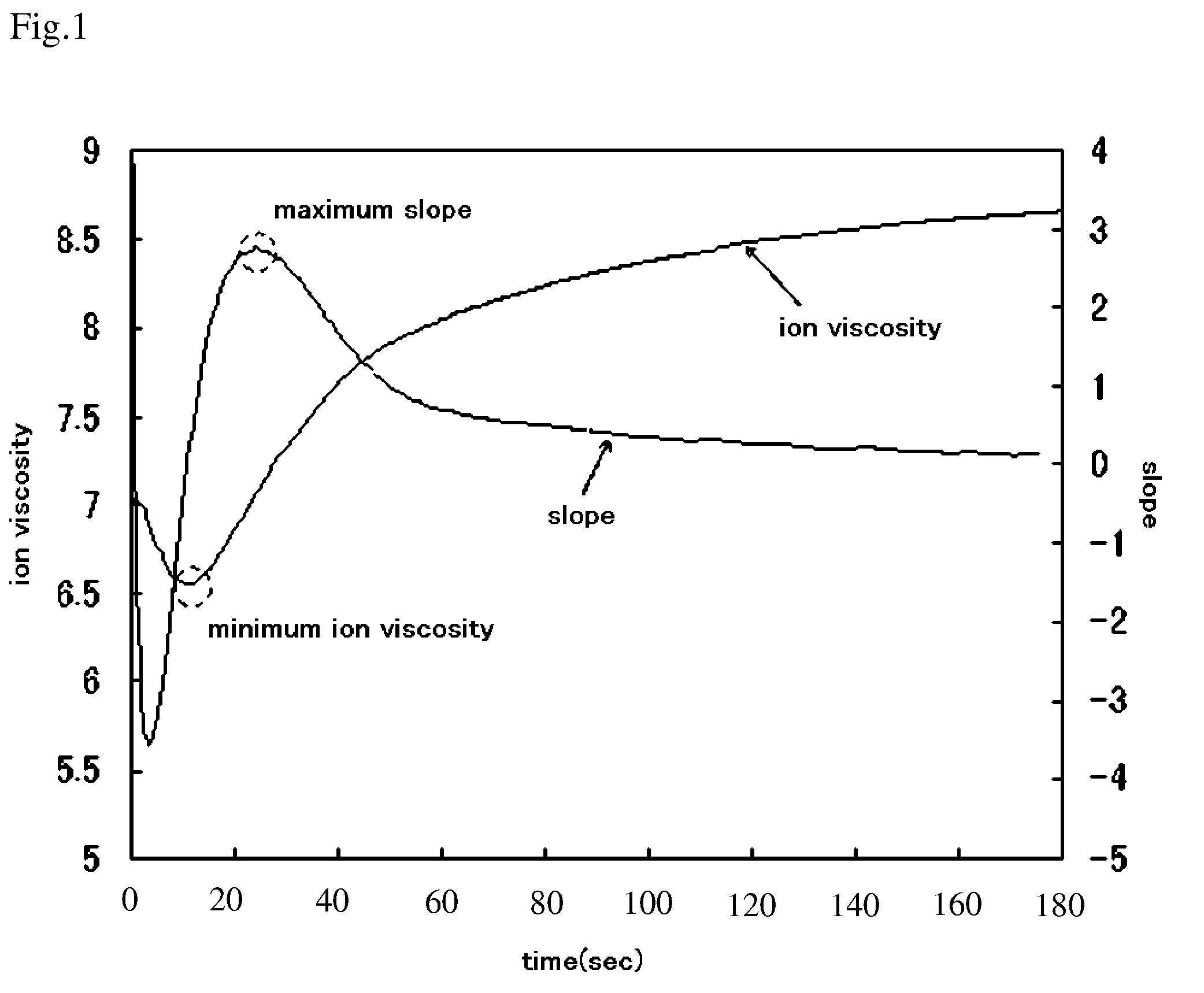
[0137]Spiral flow: The epoxy resin composition was transfered into a mold for a spiral flow measurement in accordance with EMMI-1-66 at a mold temperature of 175° C., at an transfer pressure of 6.9 MPa, and with a curing time of 120 seconds using a low-pressure transfer molding machine (KTS-15, manufactured by Kohtaki Precision Machine Co., Ltd.) to measure the flow length. The spiral flow is a parameter of flowability, and a larger value of the spiral flow means better flowability. The spiral flow is given in units of centimeters (cm).[0138]Minimum ion viscosity: A DEA231 / 1 cure analyzer manufactured by NETZSCH was used as ...
PUM
| Property | Measurement | Unit |
|---|---|---|
| frequency | aaaaa | aaaaa |
| temperature | aaaaa | aaaaa |
| softening point | aaaaa | aaaaa |
Abstract
Description
Claims
Application Information