Nitride semiconductor light emitting device

a light-emitting device and nitride technology, which is applied in the direction of semiconductor devices, basic electric elements, electrical appliances, etc., can solve the problems of reducing the brightness affecting the reliability of the light-emitting device, and entanglement of the crystal structure of the semiconductor, etc., to achieve the effect of high brightness, low crystal defect density and superior esd resistan

Active Publication Date: 2008-10-16
SAMSUNG ELECTRONICS CO LTD
View PDF3 Cites 113 Cited by
  • Summary
  • Abstract
  • Description
  • Claims
  • Application Information

AI Technical Summary

Benefits of technology

[0009]An aspect of the present invention provides a high-quality nitride semiconductor light emitting device having low crystal defect density in a nitride semiconductor crystal. An aspect of the present invention also provides a nitride semiconductor light emitting device ensuring high brightness and superior ESD resistance.

Problems solved by technology

However, typically, the nitride semiconductor such as GaN layer grown on a heterogeneous substrate such as a sapphire substrate entails many crystal defects due to lattice mismatch with the heterogeneous substrate.
These defects seriously undermine reliability of the light emitting device, for example, resistance to electrostatic discharge (ESD).
Besides, such defects absorb light to degrade brightness of the light emitting device.
However, the various attempts have entailed a complicated process such as deposition of a SiO2 mask and high costs.
However, the buffer layer 13, even when employed, does not sufficiently resolve crystal defects in the light emitting device 10.
Still, considerable density defects remain in a nitride semiconductor crystal, notably in the active layer.
These defects absorb light and hinder light emission in the active layer.
These crystal defects accordingly deteriorate brightness and reliability of the light emitting device.

Method used


Image

  • Nitride semiconductor light emitting device
  • Nitride semiconductor light emitting device
  • Nitride semiconductor light emitting device

Examples


first embodiment

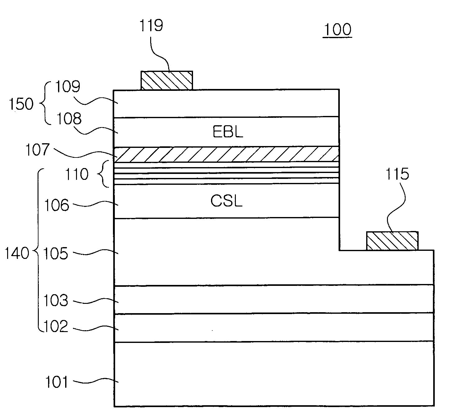
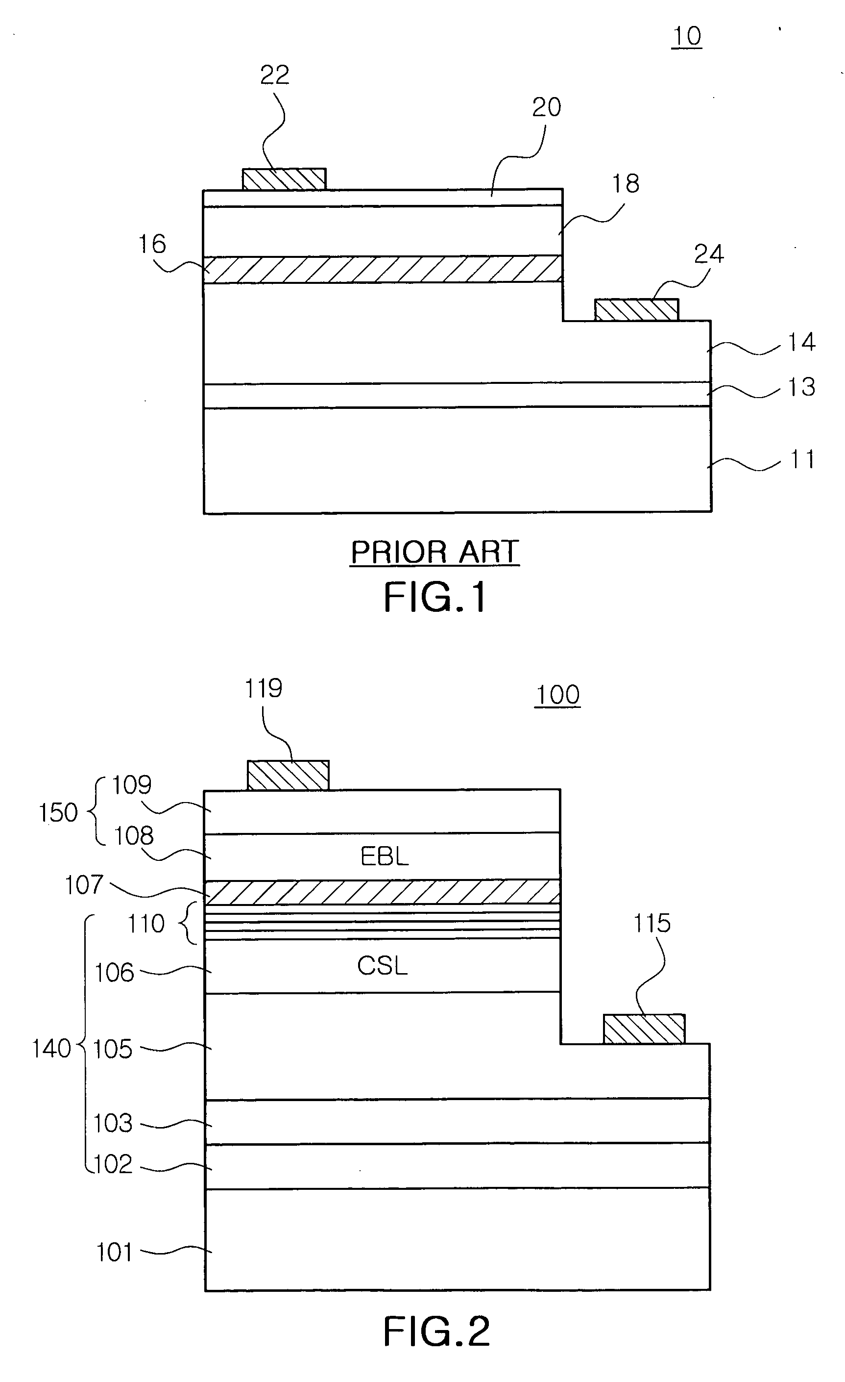
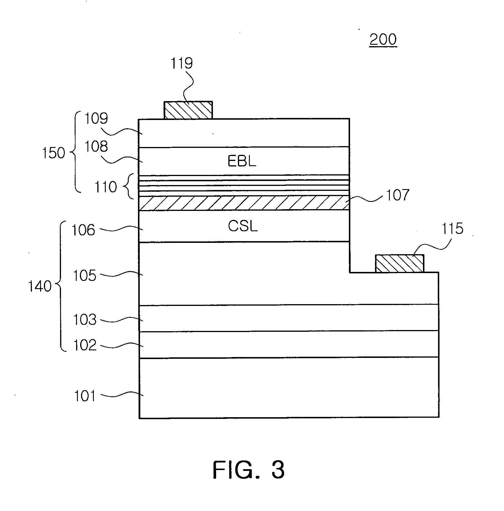
[0065]FIG. 9 is a partial cross-sectional view illustrating an intermediate layer of a multi-layer structure according to a first embodiment of the invention and FIG. 10 is a graph illustrating an exemplary band gap profile of the intermediate layer of a multi-layer structure shown in FIG. 9. In FIG. 9, a substrate is disposed at a bottom.

[0066]Referring to FIGS. 9 and 10, the intermediate layer 110 of a multi-layer structure includes a stack having an AlGaN layer 110a, a GaN layer 110b and an InGaN layer 110c deposited sequentially. Particularly, the AlGaN layer 110a / GaN layer 110b / InGaN layer 110c stack is repeatedly deposited. In the present embodiment, the AlGaN layer 110a / GaN layer 110b / InGaN layer 110c form one period of the multi-layer structure. The intermediate layer 110 may feature a superlattice structure. Out of nitride semiconductor layers 110a, 110b, and 110c of the intermediate layer 110, the AlGaN layer 110a has the largest band gap and the InGaN layer 110c has the s...

second embodiment

[0070]FIG. 11 is a partial cross-sectional view illustrating an intermediate layer of a multi-layer structure according to a second embodiment of the invention. FIG. 12 is a graph illustrating an exemplary band gap profile of the intermediate layer of a multi-layer structure of FIG. 11. The intermediate layer of the second embodiment is different from the intermediate layer of the first embodiment in terms of sequence of layers deposited.

[0071]Referring to FIGS. 11 and 12, the intermediate layer is formed of a structure where an InGaN layer 110c / GaN layer 110b / AlGaN layer 110a stack is sequentially deposited. Here, the layers of the intermediate layer are deposited in a different sequence from those of the first embodiment of FIG. 5. In the present embodiment, the InGaN layer 110c / GaN layer 110b / AlGaN layer 110a form one period of the multi-layer structure. The intermediate layer 110 may be formed of a superlattice structure.

[0072]In the same manner as the first embodiment, the mult...

third embodiment

[0073]FIG. 13 is a partial cross-sectional view illustrating an intermediate layer of a multi-layer structure according to a third embodiment of the invention. FIG. 14 is a graph illustrating an exemplary band gap profile of an intermediate layer of a multi-layer structure. In the present embodiment, a GaN layer is inserted between an AlGaN layer and an InGaN layer to prevent direct contact between AlGaN layer / InGaN layers.

[0074]Referring to FIGS. 13 and 14, the intermediate layer is formed of a structure where an AlGaN layer 110a / GaN layer 110b / InGaN layer 110c / GaN layer 110b stack is repeatedly and periodically deposited. That is, the AlGaN layer 110a / GaN layer 110b / InGaN layer 110c / GaN layer 110b form one period of the multi-layer structure. Particularly, the intermediate layer 110 features a superlattice structure. As shown in FIG. 14, the GaN layer 110b is inserted between the AlGaN layer 110a with a large band gap and the InGaN layer 110c with a small band gap to prevent direc...


PUM


Abstract

There is provided a nitride semiconductor light emitting device including: an n-type semiconductor region; an active layer formed on the n-type semiconductor region; a p-type semiconductor region formed on the active layer; an n-electrode disposed in contact with the n-type semiconductor region; a p-electrode formed on the p-type semiconductor region; and at least one intermediate layer formed in at least one of the n-type semiconductor region and the p-type semiconductor region, the intermediate layer disposed above the n-electrode, wherein the intermediate layer is formed of a multi-layer structure where at least three layers with different band gaps from one another are deposited, wherein the multi-layer structure includes one of an AlGaN layer / GaN layer / InGaN layer stack and an InGaN layer / GaN layer / AlGaN layer stack.

Description

CROSS-REFERENCE TO RELATED APPLICATIONS[0001]This application claims the priority of Korean Patent Application No. 2007-0037129 filed on Apr. 16, 2007, in the Korean Intellectual Property Office, the disclosure of which is incorporated herein by reference.BACKGROUND OF THE INVENTION[0002]1. Field of the Invention[0003]The present invention relates to a nitride semiconductor light emitting device, and more particularly, to a semiconductor light emitting device reduced in crystal defects and improved in brightness and electrostatic discharge resistance.[0004]2. Description of the Related Art[0005]Recently, a group III-V nitride semiconductor such as GaN layer, or simply a nitride semiconductor has been highlighted as a core material for a light emitting device such as a light emitting diode (LED) or a laser diode (LD) due to superior physical and chemical properties thereof. The group III-V nitride is typically formed of a semiconductor material having a composition expressed by InxAl...

Claims


Application Information

Patent Timeline
Patent Type & Authority Applications(United States)
IPC IPC(8): H01L33/00H01L33/04H01L33/14H01L33/32
CPCH01L33/06H01L33/30H01L33/12
Inventor HAN, SANG HEONKANG, SANG WONOH, JEONG TAKSEO, SEUNG BEOMKIM, DONG JOONSHIM, HYUN WOOK
Owner SAMSUNG ELECTRONICS CO LTD
Why Eureka
Try Eureka