Power Converter

Active Publication Date: 2008-10-16
KK TOSHIBA
View PDF7 Cites 12 Cited by
  • Summary
  • Abstract
  • Description
  • Claims
  • Application Information

AI Technical Summary

Benefits of technology

[0036]a high-speed auxiliary diode whose reverse recovery time is shorter than that of the free-wheel diodes; that changes over the main circuit switching elements and has a rest period of short time in which both main circuit switching elements are turned OFF when the set of a pair of main circuit switching elements mutually change over their ON condition and OFF condition; and

Problems solved by technology

Furthermore, during reverse recovery of the free-wheel diodes, the current of the main circuit temporarily flows to the low-voltage DC voltage power source 8 of the reverse voltage application circuit, so there is considerable voltage fluctuation of the auxiliary power source.

Method used


Image

  • Power Converter
  • Power Converter
  • Power Converter

Examples


first embodiment

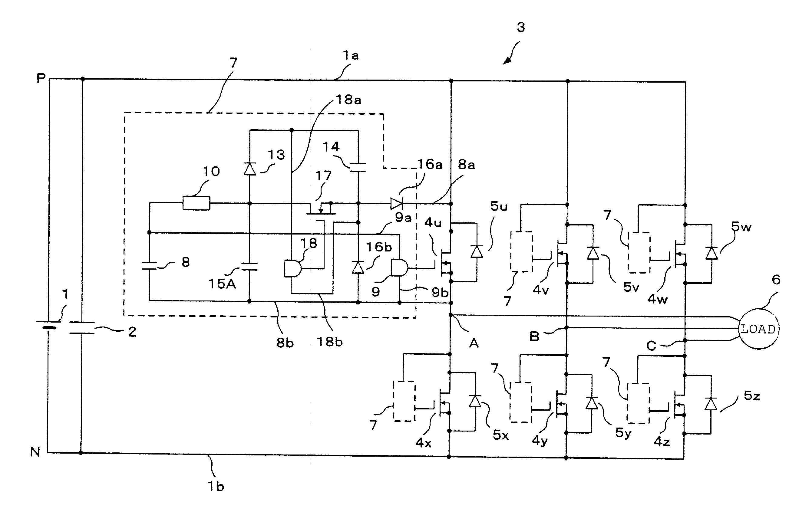
[0062]FIG. 4 is a circuit diagram of a power conversion device according to a first embodiment of the present invention. In this first embodiment, compared with the prior art example shown in FIG. 3, there is additionally provided a current suppression circuit 10 that suppresses the main circuit current flowing to the low-voltage DC voltage power source 8 during reverse recovery of the free-wheel diodes 5 (5u, 5v, 5w, 5x, 5y, 5z) in the reverse voltage application circuit 7 and a high frequency capacitor 15A that has low internal impedance even in the high frequency band is connected in parallel with the series circuit of the low-voltage DC voltage power source 8 and current suppression circuit 10. Elements which are the same as in the case of FIG. 3 are given the same reference symbols and repeated description is dispensed with.

[0063]In FIG. 4, the voltage at the point A of the main inverter circuit 3 is detected and, when it is found that a condition exists in which reverse recove...

second embodiment

[0074]FIG. 7 is a circuit diagram of major parts of a reverse voltage application circuit 7 in a power conversion device according to a second embodiment of the present invention. In this second embodiment, in comparison with the first embodiment shown in FIG. 4, the low-voltage DC voltage power source 8 is arranged to be employed as a drive power source of the main circuit switching elements 4.

[0075]In FIG. 7, the base drive circuit 9 of a main current switching element 4 comprises a gate drive amplifier 27 and gate resistance 19; the gate drive amplifier 27 obtains power from the low-voltage DC voltage power source 8 and inputs this to the gate terminal of the main circuit switching element 4 as a gate drive signal of the main circuit switching elements 4 through the gate resistance 19. FIG. 7 shows the case where a resistor is employed as the current suppression circuit 10.

[0076]Since, due to the current suppressing effect of the current suppression circuit 10 and the high freque...

third embodiment

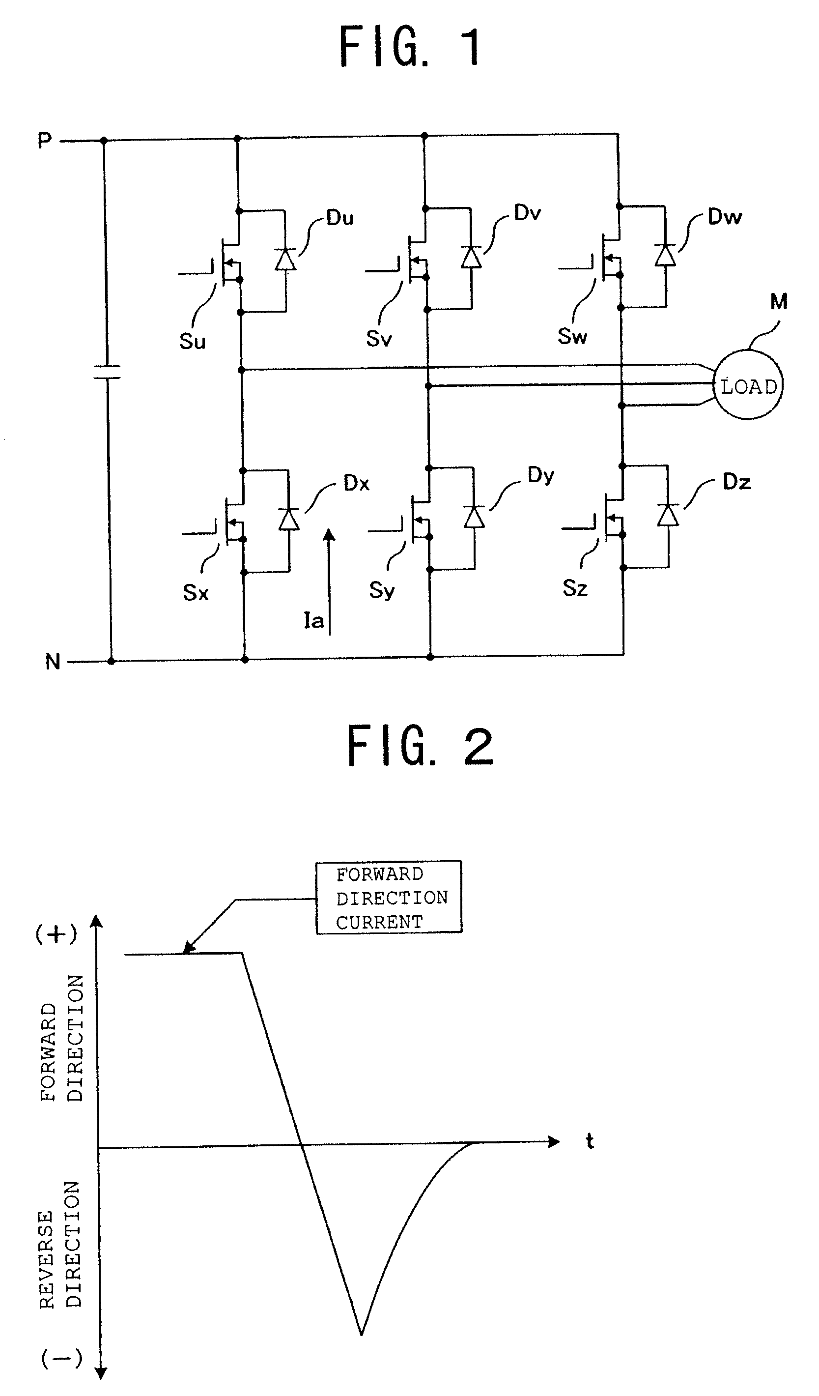
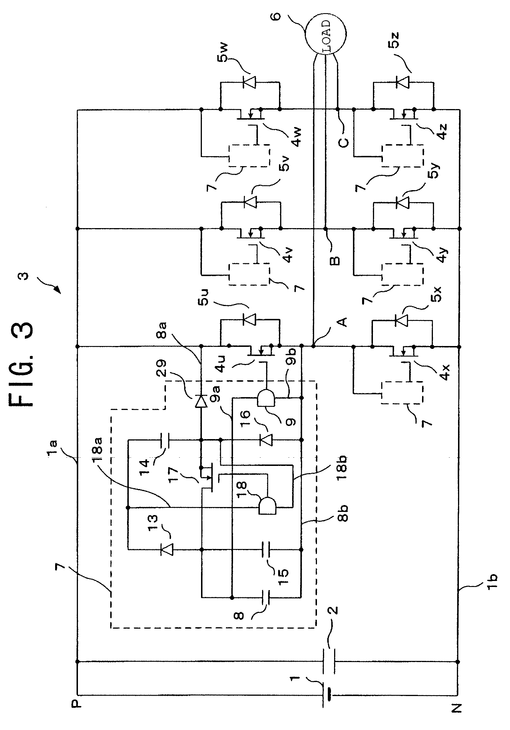
[0077]FIG. 8 is a circuit diagram of major parts of a reverse voltage application circuit 7 in a power conversion device according to a third embodiment of the present invention. In comparison with the first embodiment shown in FIG. 4, in this third embodiment, of the sets of pairs of main circuit switching elements 4u to 4w, 4x to 4z, a reverse voltage application circuit 7 is provided only for the main circuit switching elements 4x to 4z on the side that is connected with the negative side of the DC power source. FIG. 8 shows the power conversion device in the case where this is used as a three-phase inverter.

[0078]In FIG. 8, the positive side DC bus 1a and negative side DC bus 1b extend from the DC voltage source 1, IGBTs (Insulated Gate Bipolar Transistor) are employed for the positive side main circuit switching elements 4u to 4w between the positive side DC bus 1a and negative side DC bus 1b, and MOSFETs are employed for the negative side main circuit switching elements 4x to ...


PUM


Abstract

There are provided: sets of pairs of main circuit switching elements (4u), (4x) that supply power to a load, connected in series with a DC power source; free-wheel diodes (5u), (5x) connected in anti-parallel with these main circuit switching elements; and a reverse voltage application circuit (8) that applies reverse voltage smaller than the DC voltage source to the free-wheel diodes when these free-wheel diodes cut off. The reverse voltage application circuit includes a current suppression circuit (10) that suppresses the main circuit current flowing in the low-voltage DC voltage power source on reverse recovery of the free-wheel diodes.

Description

TECHNICAL FIELD[0001]The present invention relates to a power conversion device constructed by connecting free-wheel diodes in anti-parallel with main circuit switching elements.BACKGROUND ART[0002]In a known inverter device construction, as shown in FIG. 1, free-wheel diodes Du to Dw and Dx to Dz are connected in anti-parallel with MOSFETs Su to Sw and Sx to Sz. In this construction, when the MOSFETs Su to Sw and Sx to Sz are turned OFF, the current energy accumulated in the load M is fed back through the free-wheel diodes Du to Dw and Dx to Dz.[0003]In this case, when for example the MOSFET Su is turned ON when a forward current Ia flows in the free-wheel diode Dx, the PN voltage (so-called DC link voltage) is applied as reverse bias to both terminals of the free-wheel diode Dx, with the result that, as shown in FIG. 2, a reverse-direction current due to the residual charge flows in the free-wheel diode Dx before the free-wheel diode Dx cuts off. Considerable loss was therefore ge...

Claims


Application Information

Patent Timeline
IPC IPC(8): H02M7/538H02M7/5387H02M7/00H02M7/5388
CPCH02M1/34H02M7/5387H02M2001/0051H02M2001/344Y02B70/1491Y02B70/10H02M1/0051H02M1/344
Inventor MOCHIKAWA, HIROSHIKOYAMA, TATEO
Owner KK TOSHIBA
Why Eureka
Try Eureka