Photovoltaics on silicon

Active Publication Date: 2008-10-23
TAIWAN SEMICON MFG CO LTD
View PDF113 Cites 172 Cited by
  • Summary
  • Abstract
  • Description
  • Claims
  • Application Information

AI Technical Summary

Benefits of technology

[0005]Aspect ratio trapping (ART) technology enables the growing of high quality lattice-mismatched materials such as Ge or GaAs (or other III-V materials) on Si substrates, as described in U.S. patent application Ser. Nos. 11/436,198, 11/728,032, and 11/852,078, all incorporated by reference herein. Using Si substrates and ART technology to provide relatively high quality Ge or GaAs layers allows for building PVDs that have the advantages of Si substrates (e.g., cost, manufacturing, thermal performance, radiation resistance, strength) as well as advantages of PVDs built u

Problems solved by technology

However, the fundamental material incompatibility issues between III-V compounds and Si still represent a substantial hurdle for achieving high-performance Si-based III-V PV cells.
These material incompatibility issues include lattice mismatch between III-V compounds and Si and a large mismatch in thermal expansion coefficiency.
The high density of dislocations that occur at interfaces between Si and III-V compounds le

Method used


Image

  • Photovoltaics on silicon
  • Photovoltaics on silicon
  • Photovoltaics on silicon

Examples


Embodiment Construction

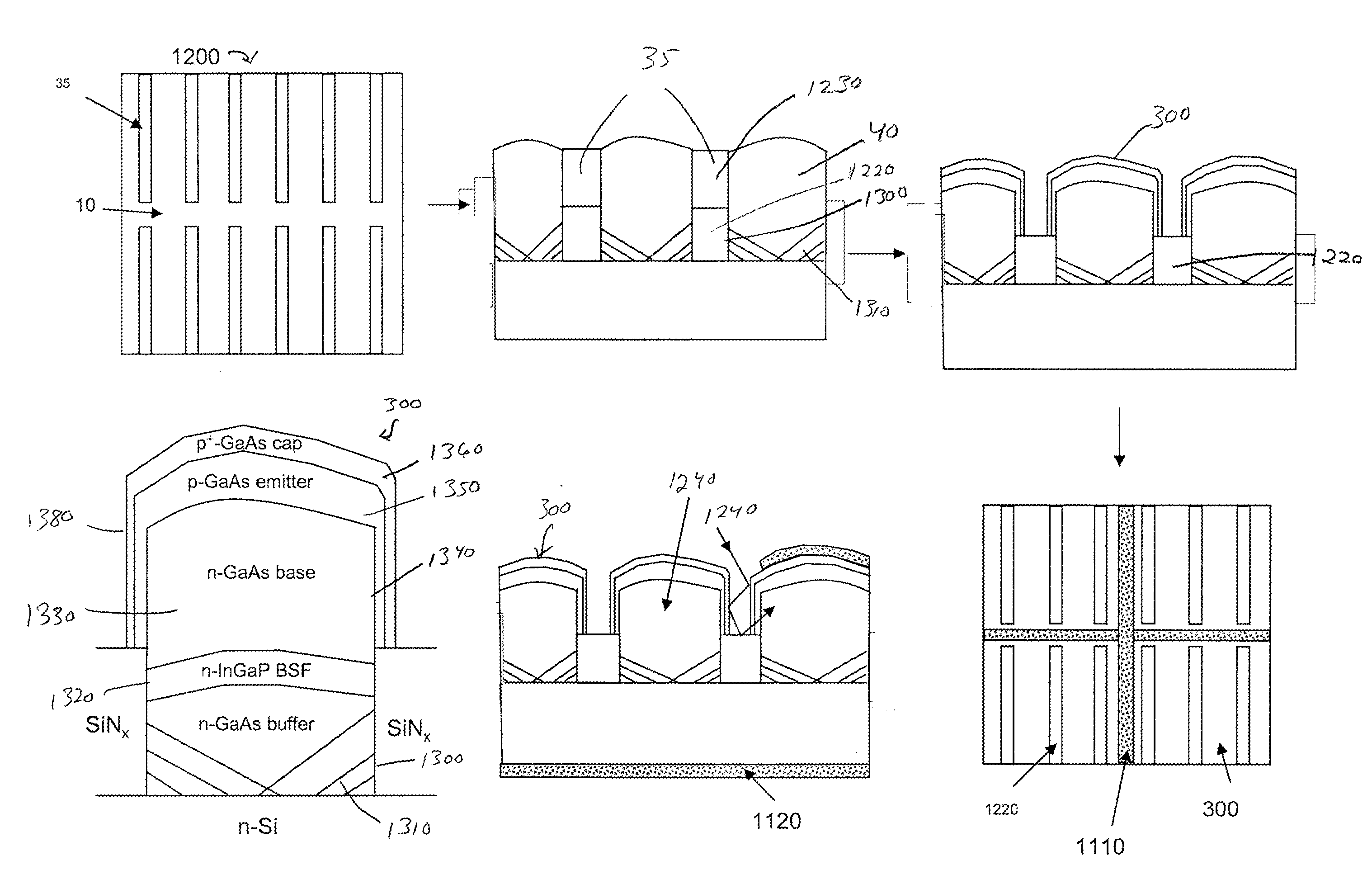
[0048]A significant feature of embodiments of the present invention is the provision of a pathway to overcome the material incompatibility between lattice-mismatched materials, such as III-V compounds formed on a Si substrate. This approach is based on ART technology for selective epitaxy. See, e.g., U.S. patent application Ser. No. 11 / 436,062.

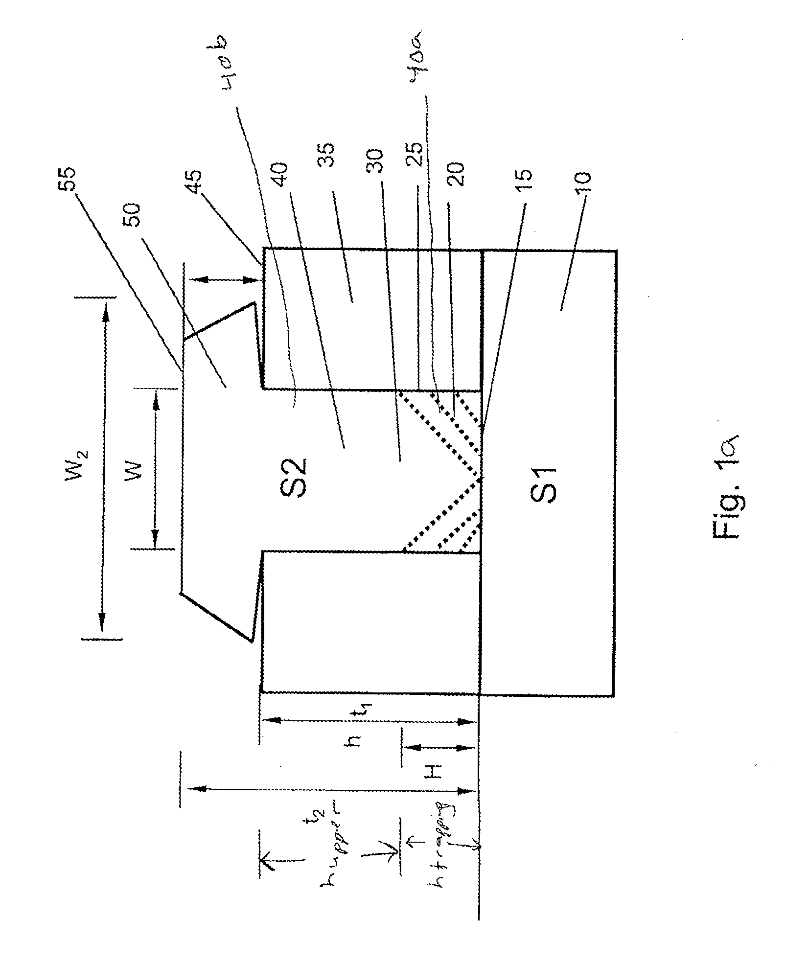
[0049]Referring to FIGS. 1a and 1b, an insulating material such as SiO2, is used to define openings, e.g., trenches, above a semiconductor substrate. Semiconductor substrate may include, e.g., silicon. The openings are configured using ART techniques so that when a lattice-mismatched material, e.g., GaAs is epitaxially grown, defects in the lattice-mismatched GaAs layer are trapped in the lower region of the trenches and the GaAs region at the top of the trenches is relatively defect free.

[0050]More specifically, a substrate 10 includes a first crystalline semiconductor material S1. The substrate 10 may be, for example, a bulk silicon wafer, a...


PUM


Abstract

Structures including crystalline material disposed in openings defined in a non-crystalline mask layer disposed over a substrate. A photovoltaic cell may be disposed above the crystalline material.

Description

RELATED APPLICATIONS[0001]This application claims the benefit of and priority to U.S. Provisional Application Ser. No. 60 / 7922,533 filed Apr. 9, 2007, the disclosure of which is hereby incorporated by reference in its entirety.FIELD OF THE INVENTION[0002]The technology disclosed herein relates generally to photovoltaic devices (PVDs).BACKGROUND AND SUMMARY[0003]Conventional PVDs generally fall into two categories—a first type that uses Si substrates and Si-based materials for active photovoltaic (PV) regions and a second type that uses Ge or GaAs substrates with one or more active PV regions constructed using lattice-matched III-V compound semiconductor materials. Conventional Si-based PVDs generally have lower conversion efficiency than PVDs based on Ge or GaAs substrates (e.g., 10-15% vs. 20-40%). Si-based PVDs are less expensive to make than Ge or GaAs-based PVDs. PVDs built on Si substrates generally cost less than PVDs built on Ge or GaAs substrates. But PVDs built on Ge or GaA...

Claims


Application Information

Patent Timeline
IPC IPC(8): H01L31/00
CPCH01L31/0693H01L31/1852Y02E10/544Y02E10/546Y02E10/547Y02P70/50H01L21/0262H01L31/035281H01L31/047H01L31/0687H01L31/184H01S2304/12
Inventor LI, JIZHONGLOCHTEFELD, ANTHONY J.SHEEN, CALVINCHENG, ZHIYUAN
Owner TAIWAN SEMICON MFG CO LTD
Why Eureka
Try Eureka