Thin film transistor including selectively crystallized channel layer and method of manufacturing the thin film transistor

a thin film transistor and selective crystal technology, applied in the field of thin film transistors including selective crystallization channel layers and manufacturing methods, can solve the problems of difficult to increase the operating speed of a liquid crystal display, low charge carrier mobility of channel layers, etc., and achieve low off-current operation, stable contact characteristics, and high charge carrier mobility

Active Publication Date: 2008-10-23
SAMSUNG ELECTRONICS CO LTD
View PDF75 Cites 4009 Cited by
  • Summary
  • Abstract
  • Description
  • Claims
  • Application Information

AI Technical Summary

Benefits of technology

[0010]The present invention provides a reliable thin film transistor (TFT) having stable contact characteristics for high charge carrier mobility and low off-current operation.

Problems solved by technology

However, when amorphous Si is used for forming channel layers of TFTs, the charge carrier mobility of the channel layers is low (0.5 cm2 / Vs).
Therefore, it is difficult to increase the operating speed of a liquid crystal display when TFTs having amorphous-Si channel layers are used as switching devices in a liquid crystal display.

Method used


Image

  • Thin film transistor including selectively crystallized channel layer and method of manufacturing the thin film transistor
  • Thin film transistor including selectively crystallized channel layer and method of manufacturing the thin film transistor
  • Thin film transistor including selectively crystallized channel layer and method of manufacturing the thin film transistor

Examples


first embodiment

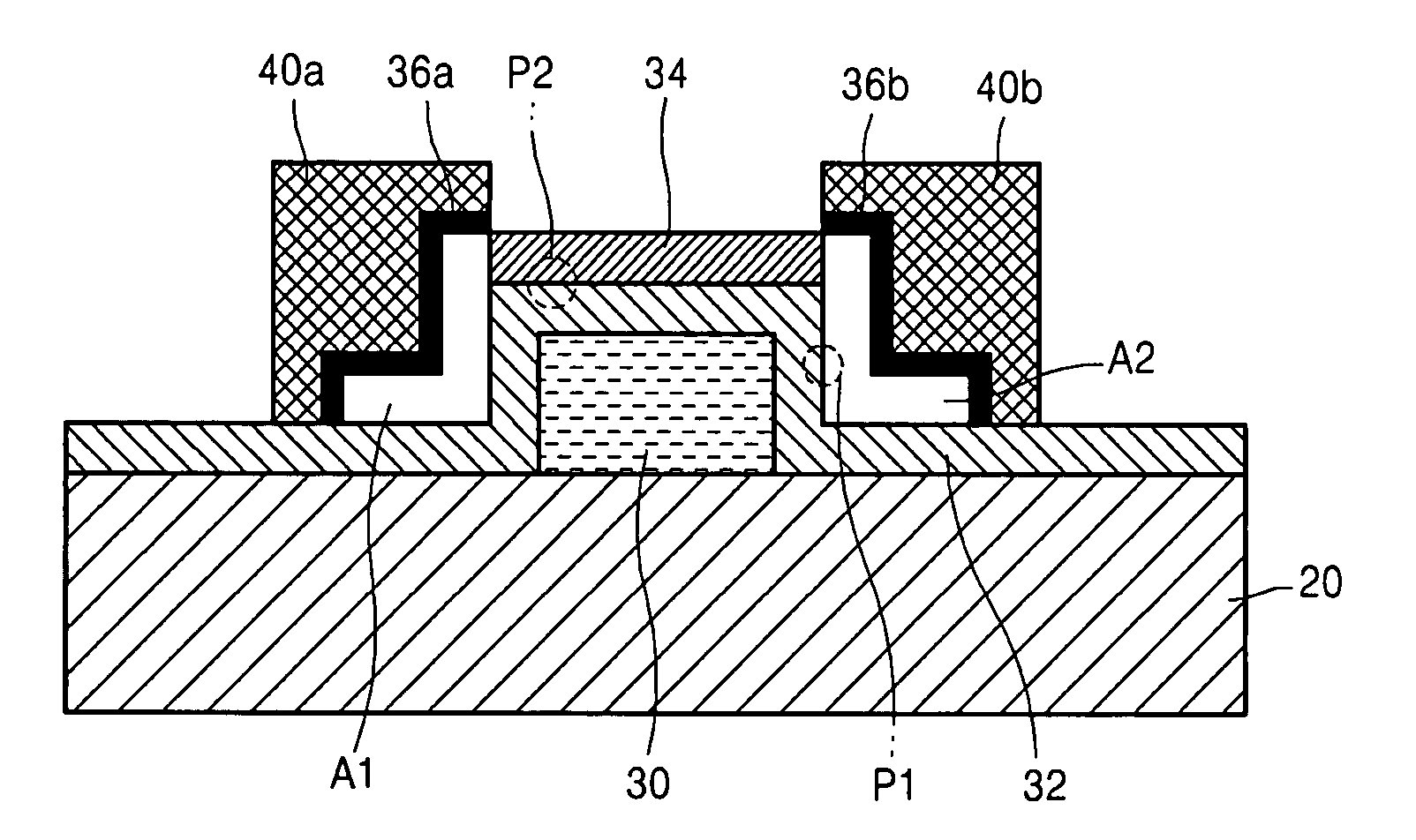
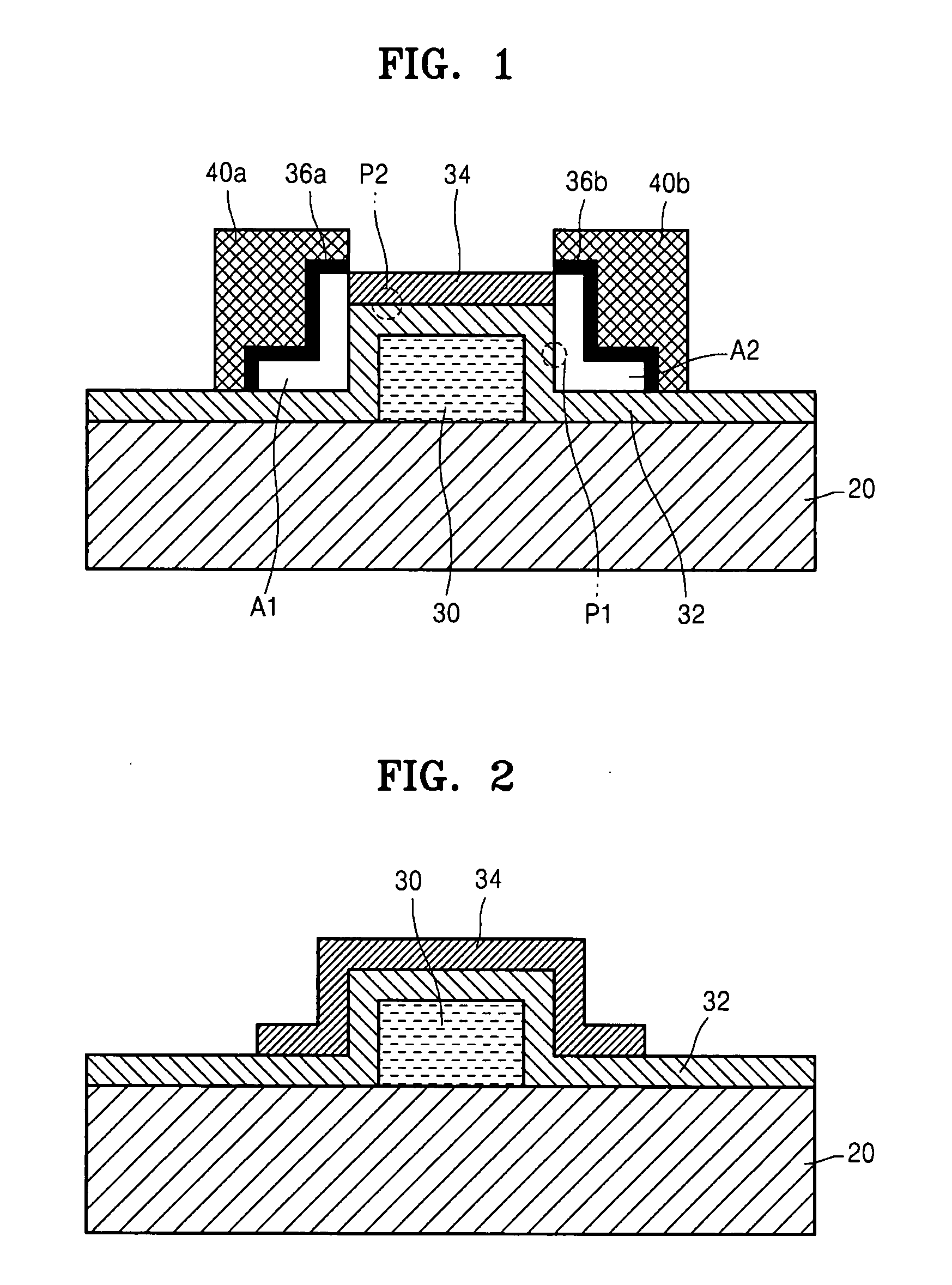
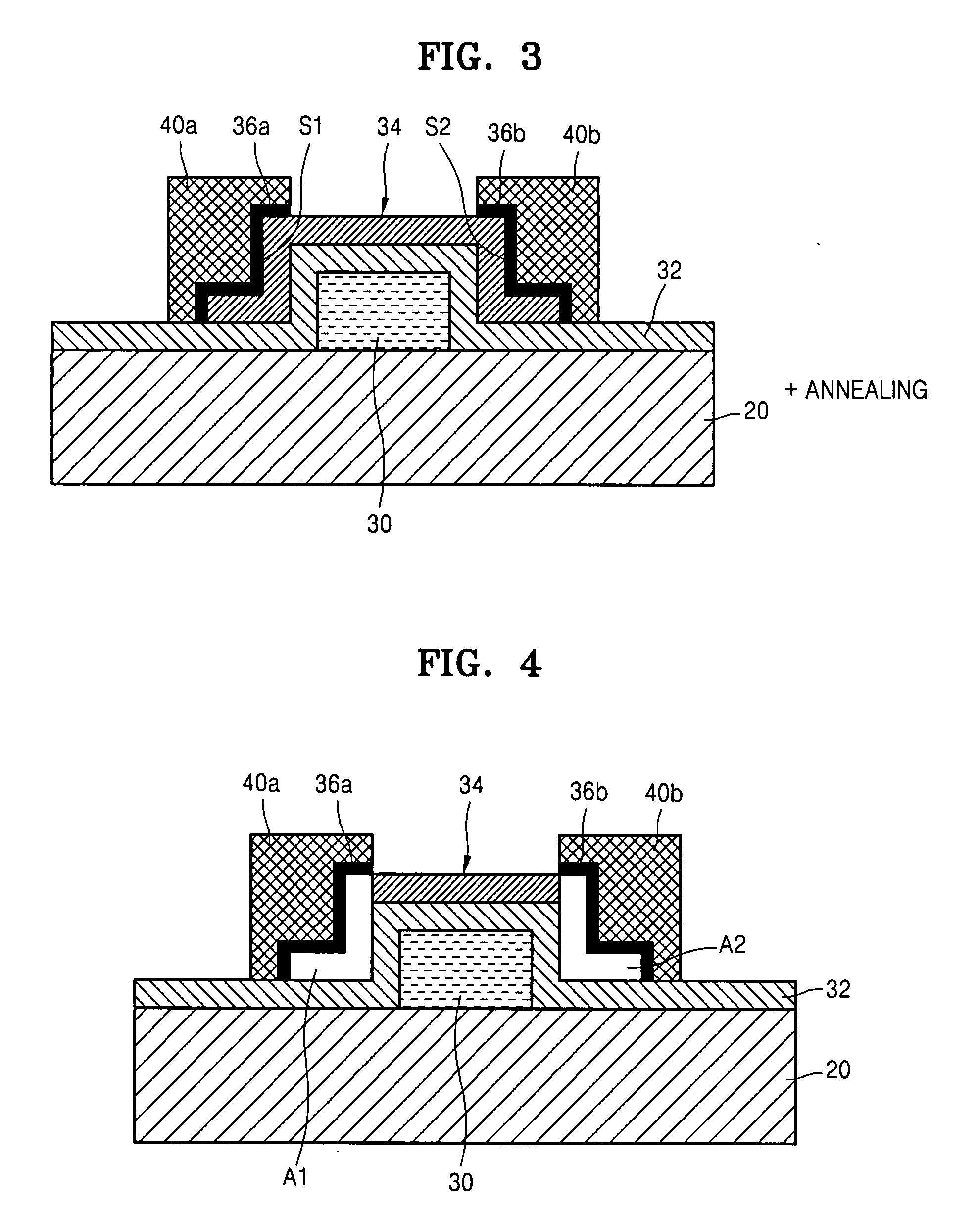
[0049]Referring to FIG. 2, a gate 30 is formed on a substrate 20. The substrate 20 may be an insulation substrate. For example, the substrate 20 may be a glass substrate or a semiconductor substrate including an insulation layer thereon. The gate 30 may be formed of molybdenum (Mo). Alternatively, the gate 30 can be formed of other conductive materials. A gate insulation layer 32 is formed on the substrate 20 to cover top and side surfaces of the gate 30. The gate insulation layer 32 may be formed of a silicon oxide. A channel layer 34 is formed on the gate insulation layer 32. The channel layer 34 may be formed of an amorphous oxide semiconductor. For example, the channel layer 34 may be formed of a(In203).b(Ga203).c(ZnO) (where a, b, and c are real numbers, and a≧0, b≧0, and c>0).

[0050]A metal layer (not shown) and an electrode layer (not shown) are sequentially formed on the gate insulation layer 32 to cover the channel layer 34. The metal layer may be formed of a metal which can...

second embodiment

[0057]In the current embodiment, only the surface of the channel layer 34 is crystallized by the ion implantation.

[0058]In the following description, like reference numerals in the drawings denote like elements.

[0059]Referring to FIG. 5, the operation of forming the channel layer 34 on the gate insulation layer 32 and the previous operations are the same as those of the previous embodiment described with reference to FIGS. 2 through 4. Then, a source electrode 46a is formed on the gate insulation layer 32 to cover one side portion of the channel layer 34, and a drain electrode 46b is formed on the gate insulation layer 32 to cover the other side portion of the channel layer 34. The source and drain electrodes 46a and 46b may correspond in material and position to the source and drain electrodes 40a and 40b of the previous embodiment.

[0060]Referring to FIG. 6, a metal component 48 is implanted into the channel layer 34 through an opening between the source and drain electrodes 46a an...

third embodiment

[0064]In the current embodiment, the surface of the channel layer 34 is crystallized without using ion implantation.

[0065]Referring to FIG. 9, the operation of forming the source and drain electrodes 46a and 46b and the previous operations are the same as those of the previous embodiment described with reference to FIG. 5. Then, a metal layer 54 is formed above the gate insulation layer 32 to cover the source and drain electrodes 46a and 46b and the top surface of the channel layer 34 exposed between the source and drain electrodes 46a and 46b. For example, the metal layer 54 may be formed of titanium (Ti).

[0066]Thereafter, the metal layer 54 and the channel layer 34 are annealed. The annealing of the metal layer 54 and the channel layer 34 may be performed in the same manner as that performed in the previous embodiment. During the annealing, a metal component of the metal layer 54 is diffused into the channel layer 34. Then, if the metal layer 54 remains after the annealing, the re...


PUM


Abstract

Provided are a thin film transistor (TFT) including a selectively crystallized channel layer, and a method of manufacturing the TFT. The TFT includes a gate, the channel layer, a source, and a drain. The channel layer is formed of an oxide semiconductor, and at least a portion of the channel layer contacting the source and the drain is crystallized. In the method of manufacturing the TFT, the channel layer is formed of an oxide semiconductor, and a metal component is injected into the channel layer so as to crystallize at least a portion of the channel layer contacting the source and the drain. The metal component can be injected into the channel layer by depositing and heat-treating a metal layer or by ion-implantation.

Description

CROSS-REFERENCE TO RELATED PATENT APPLICATION[0001]This application claims the benefit of Korean Patent Application No. 10-2007-0038978, filed on Apr. 20, 2007, in the Korean Intellectual Property Office, the disclosure of which is incorporated herein in its entirety by reference.BACKGROUND OF THE INVENTION[0002]1. Field of the Invention[0003]The present invention relates to a semiconductor device, and more particularly, to a thin film transistor (TFT) including a selectively crystallized channel layer and a method of manufacturing the TFT.[0004]2. Description of the Related Art[0005]TFTs are used for static random access memories (SRAMs) and read only memories (ROMs). Particularly, TFTs are widely used as pixel driving devices in active matrix flat panel displays. For example, TFTs are used as switching devices or current driving devices in liquid crystal displays or organic electro-luminescence displays.[0006]When TFTs are used as switching devices, the TFTs protect pixels from el...

Claims


Application Information

Patent Timeline
Patent Type & Authority Applications(United States)
IPC IPC(8): H01L29/04H01L21/34
CPCH01L21/02554H01L21/02565H01L21/02667H01L21/02672H01L21/02675H01L29/7869
Inventor LEE, EUN-HAKANG, DONG-HUNLEE, JAE-CHEOLKIM, CHANG-JUNGLIM, HYUCK
Owner SAMSUNG ELECTRONICS CO LTD
Why Eureka
Try Eureka