
Oscillator circuit and semiconductor device including the same

a technology of oscillator circuit and oscillator frequency, which is applied in the direction of pulse generator, pulse manipulation, pulse technique, etc., can solve the problems of difficult to stabilize oscillation frequency and circuit malfunction, and achieve low noise, less fluctuation, and high reliability

Inactive Publication Date: 2008-10-23
SEMICON ENERGY LAB CO LTD
View PDF17 Cites 6 Cited by
  • Summary
  • Abstract
  • Description
  • Claims
  • Application Information

AI Technical Summary

Benefits of technology

[0007]Further, in a case of obtaining a power supply voltage with the use of a radio signal such as an external radio wave or electromagnetic wave in an RFID (radio frequency identification) tag or the like which has recently attracted attention as a semiconductor device for communicating data by wireless communication, the power supply voltage fluctuates easily in accordance with a distance from a place where a signal is generated and the fluctuation in the power supply voltage changes an oscillation frequency.
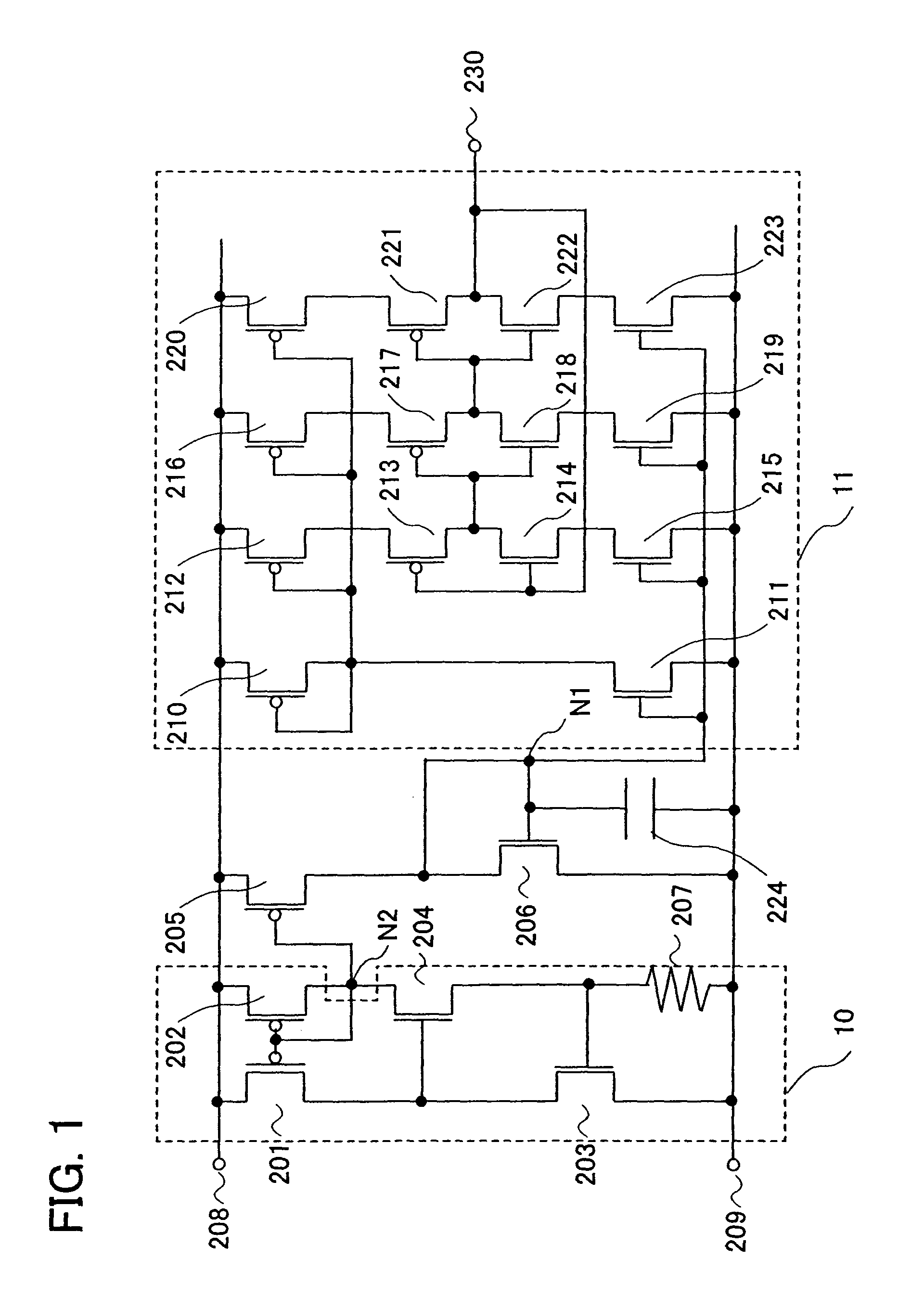
[0016]In a case where the potential difference between the power supply voltage terminals changes and the voltage of the input terminal of the voltage controlled oscillator circuit is constant, the oscillation frequency of the voltage controlled oscillator circuit fluctuates in accordance with the potential difference between the power supply voltage terminals. In the present invention, the voltage of the gate terminal of the n-channel transistor fluctuates; therefore, a fluctuation in an oscillation frequency in accordance with a potential difference between the power supply voltage terminals can be suppressed.
[0017]Note that the capacitor connected to the first node can suppress a voltage fluctuation at the first node in a case where the potential difference between the power supply voltage terminals significantly changes.
[0025]By using the present invention, an oscillator circuit which is not easily affected by a noise due to a fluctuation in power and which outputs a signal having a stable frequency with less fluctuation in a wide range of voltages. The oscillator circuit of the present invention makes it possible to generate a stable clock signal and accordingly, a semiconductor device which is highly reliable and can transmit and receive data wirelessly can be provided.

Problems solved by technology

However, a conventional oscillator circuit has the following problem.
Therefore, in a case where an output from the oscillator circuit is used as a clock signal, if the oscillation frequency fluctuates, the clock signal is changed, resulting in a circuit malfunction.
An oscillation frequency is easily affected by a ripple of a power supply voltage or a noise due to a wireless signal; therefore, it is difficult to stabilize an oscillation frequency.

Method used


Image

  • Oscillator circuit and semiconductor device including the same
  • Oscillator circuit and semiconductor device including the same
  • Oscillator circuit and semiconductor device including the same

Examples


embodiment mode 1

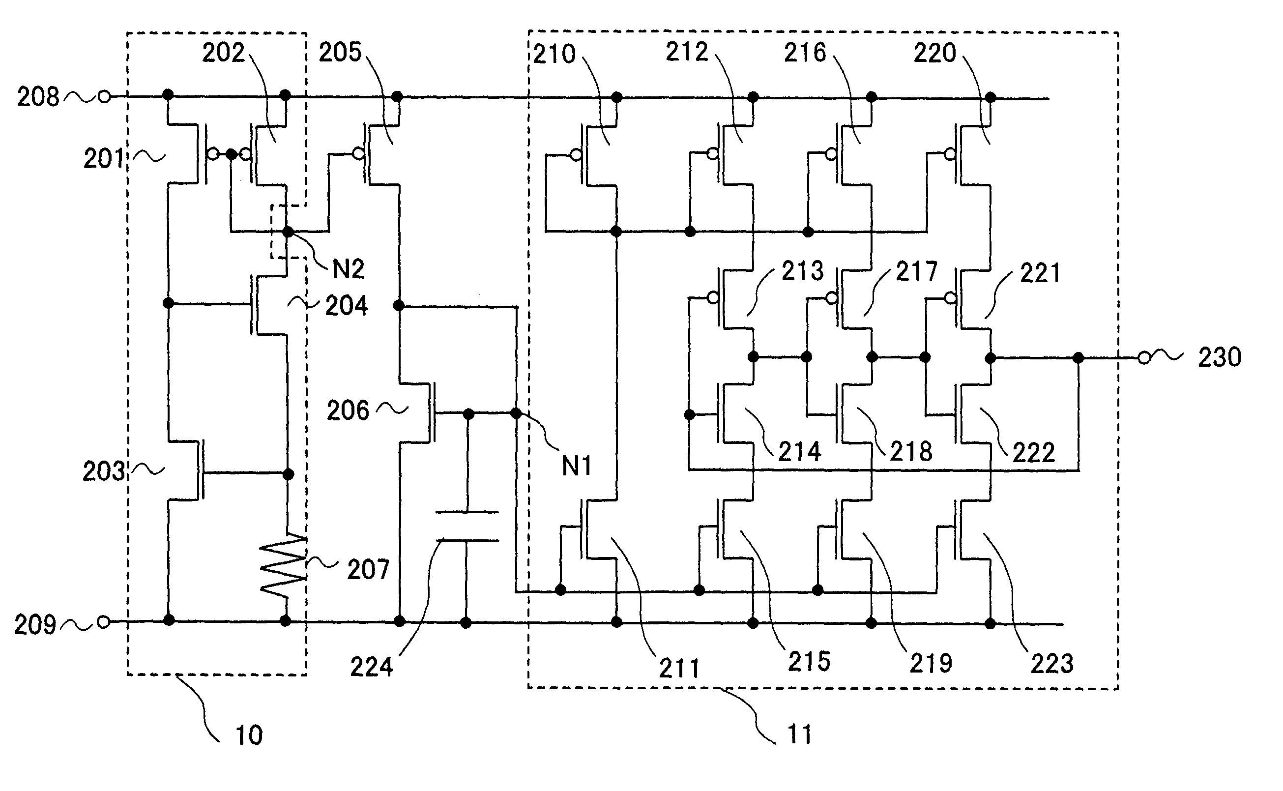
[0044]FIG. 1 shows a structure of an oscillator circuit of the present invention. In FIG. 1, a terminal 208 is an input voltage terminal and a terminal 209 is a reference voltage terminal of an input voltage. Note that in this specification, the input voltage terminal and the reference voltage terminal of an input voltage are also referred to as a first terminal and a second terminal respectively and may be collectively referred to as power supply voltage terminals. A gate electrode and a source electrode of an n-channel transistor (hereinafter referred to as NMOS) 206 are connected to a node N1 and the terminal 209, respectively. A drain electrode of a p-channel transistor (hereinafter referred to as PMOS) 205 and a drain electrode of the NMOS 206 are connected and a connection portion thereof is connected to the node N1. A source electrode and a gate electrode of the PMOS 205 are connected to the terminal 208 and a node N2, respectively. In addition, the node N1 is connected to th...

embodiment mode 2

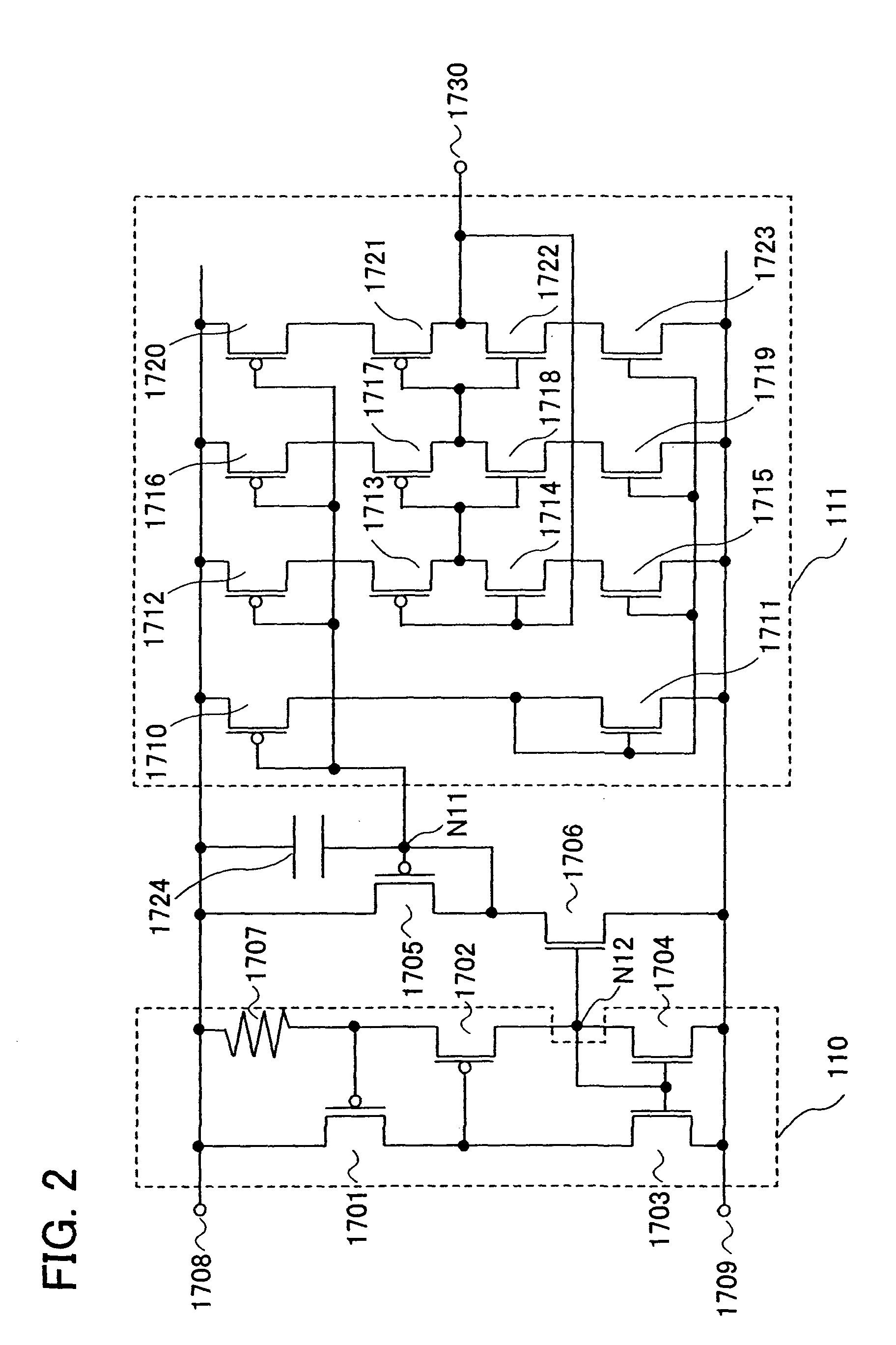
[0059]In this embodiment mode, FIG. 2 shows a structure of an oscillator circuit of the present invention, which is different from that of Embodiment Mode 1. In FIG. 2, a terminal 1708 is an input voltage terminal, and a terminal 1709 is a reference voltage terminal of an input voltage. A gate electrode and a source electrode of a PMOS 1705 are connected to a node N11 and the terminal 1708, respectively. A drain electrode of the PMOS 1705 and a drain electrode of an NMOS 1706 are connected and a connection portion thereof is connected to the node N11. A source electrode and a gate electrode of the NMOS 1706 are connected to the terminal 1709 and a node N12, respectively. The node N11 is connected to the terminal 1708 through a capacitor 1724. With a voltage of the node N12, a current flows through the NMOS 1706, and a connection between the PMOS 1705 and the NMOS 1706 allows the current to flow through the PMOS 1705 as well. When the current flows through the PMOS 1705, a voltage co...

embodiment mode 3

[0074]In this embodiment mode, a semiconductor device which has the oscillator circuit described in the above embodiment modes and can transmit and receive data wirelessly is described with reference to drawings.

[0075]In recent years, semiconductor devices each combining a micro IC chip and an antenna for wireless communication, such as RFID tags, have attracted lots of attention. An RFID tag can write and read data by transmitting and receiving a communication signal with the use of a wireless communication device (also referred to as a reader / writer). Note that an RFID tag (hereinafter simply referred to as an RFID) is also called an IC (Integrated Circuit) tag, an IC chip, an RF tag, a wireless tag, or an electronic tag.

[0076]As an application field of a semiconductor device which can transmit and receive data wirelessly, such as an RFID, product management in the distribution industry is given as an example. Product management using bar codes or the like is mainstream at present...


PUM


Abstract

A stable frequency is outputted by an oscillator circuit including a constant current circuit which is electrically connected between a first terminal and a second terminal, a voltage controlled oscillator circuit in which an oscillation frequency fluctuates in accordance with a potential difference between power supply voltage terminals, an n-channel transistor, a p-channel transistor in which a gate-source voltage is set to be constant by the constant current circuit, and a capacitor, in which a source electrode of the p-channel transistor is electrically connected to the first terminal, a drain electrode of the p-channel transistor is electrically connected a drain electrode and a gate electrode of the n-channel transistor, a source electrode of the n-channel transistor is electrically connected to the second terminal, and a gate electrode of the n-channel transistor is electrically connected to the second terminal through the capacitor.

Description

BACKGROUND OF THE INVENTION[0001]1. Field of the Invention[0002]The present invention relates to an oscillator circuit and a semiconductor device including the oscillator circuit.[0003]2. Description of the Related Art[0004]In recent years, semiconductor devices in each of which various circuits are integrated on one insulating surface have been developed. As a clock circuit necessary for a circuit, various oscillator circuits are known.[0005]Oscillator circuits have been developed using CMOSs, and an oscillator circuit using a CMOS inverter is given as a typical example (for example, Patent Document 1: Japanese Published Patent Application No. 2003-283307).SUMMARY OF THE INVENTION[0006]However, a conventional oscillator circuit has the following problem. When a power supply voltage supplied to an oscillator circuit fluctuates, the value of a current flowing through an inverter is changed and thus an oscillation frequency is changed. Therefore, in a case where an output from the osc...

Claims


Application Information

Patent Timeline
Patent Type & Authority Applications(United States)
IPC IPC(8): H03L9/00
CPCH01L27/1214H03K3/011H03K5/133H03K2005/00039H03K2005/0013H03K3/0315H01L27/1255H01L27/1266H03K3/354
Inventor MATSUZAKI, TAKANORI
Owner SEMICON ENERGY LAB CO LTD
Learn More