Film Formation Apparatus, Film Formation Method, Manufacturing Apparatus, and Method for Manufacturing Light-Emitting Device

a technology of film formation and manufacturing equipment, applied in the direction of solid-state devices, vacuum evaporation coatings, coatings, etc., can solve the problems of long time, limited improvement in productivity, difficult design as an automation process, etc., and achieve the effect of short time, large area, and short manufacturing tim

Inactive Publication Date: 2008-10-23
SEMICON ENERGY LAB CO LTD
View PDF13 Cites 65 Cited by
  • Summary
  • Abstract
  • Description
  • Claims
  • Application Information

AI Technical Summary

Benefits of technology

[0013]The present invention provides a film formation apparatus included in a manufacturing apparatus and a film formation method that reduce manufacturing cost by improvement in use efficiency of a material, which is not limited to an EL material, and are excellent in uniformity of film formation and throughput. As for the uniformity of film formation in particular, it is an object of the present invention to set a range of variations in film thickness to less than 3%.
[0014]The present invention provides a film formation apparatus which can realize the uniformity of film formation even without using a film thickness monitor.
[0015]Since evaporation is performed in a vacuum, there are problems in that evacuation of a film formation chamber takes a long time, time required for each step varies from treatment chamber to treatment chamber, and the like; thus, designing as an automation process is difficult and improvement in productivity is limited. In particular, evaporation and stacking of layers each containing an organic compound take a long time; accordingly, reducing treatment time per substrate is limited. Accordingly, it is another object of the present invention to reduce treatment time per substrate.

Problems solved by technology

Since evaporation is performed in a vacuum, there are problems in that evacuation of a film formation chamber takes a long time, time required for each step varies from treatment chamber to treatment chamber, and the like; thus, designing as an automation process is difficult and improvement in productivity is limited.
In particular, evaporation and stacking of layers each containing an organic compound take a long time; accordingly, reducing treatment time per substrate is limited.

Method used


Image

  • Film Formation Apparatus, Film Formation Method, Manufacturing Apparatus, and Method for Manufacturing Light-Emitting Device
  • Film Formation Apparatus, Film Formation Method, Manufacturing Apparatus, and Method for Manufacturing Light-Emitting Device
  • Film Formation Apparatus, Film Formation Method, Manufacturing Apparatus, and Method for Manufacturing Light-Emitting Device

Examples


embodiment mode 1

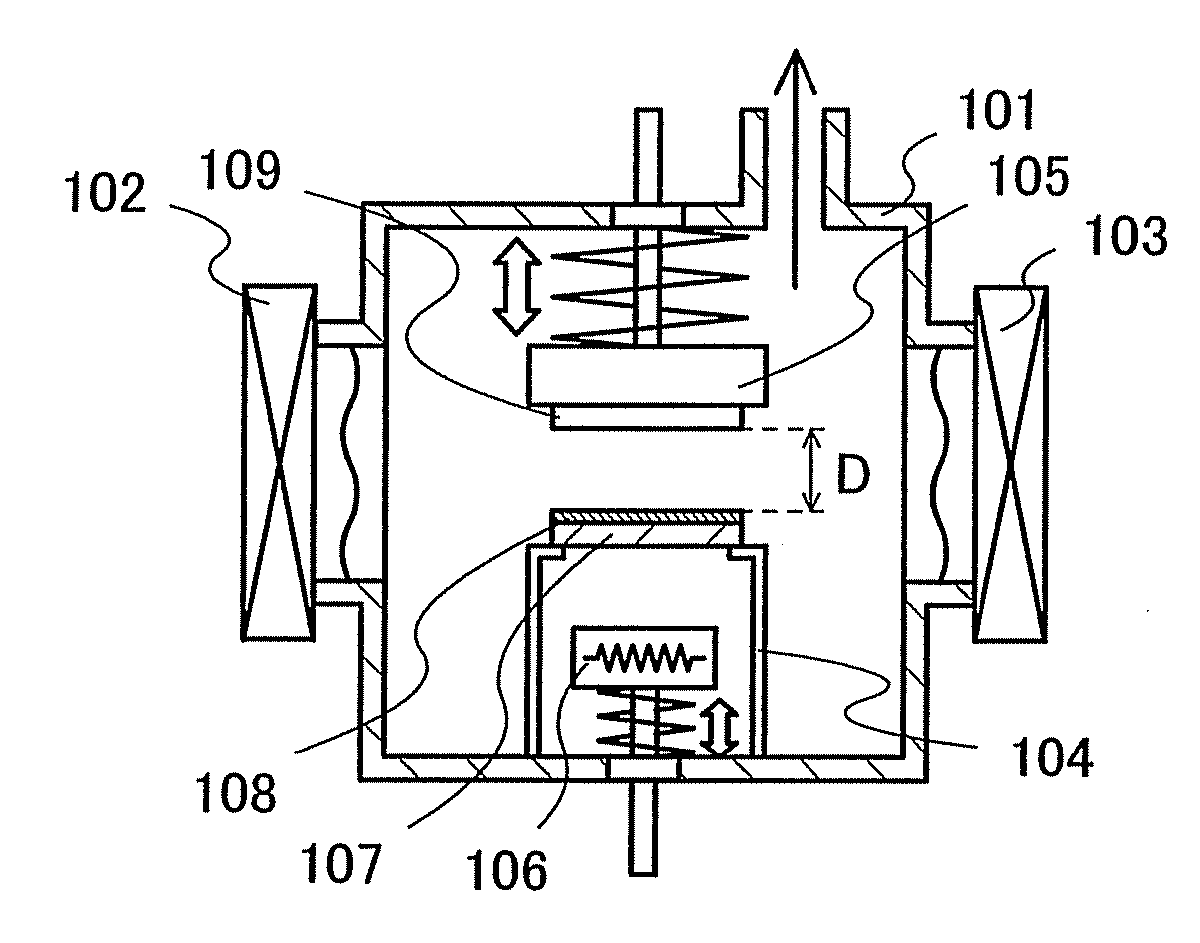
[0073]A procedure of film formation will be described with reference to FIGS. 1A to 1C that are schematic cross-sectional views of a film formation apparatus of the present invention.

[0074]In FIG. 1A, a film formation chamber 101 is a vacuum chamber and connected to other treatment chambers through a first gate valve 102 and a second gate valve 103. In the film formation chamber 101, at least, a plate supporting mechanism which is a first substrate supporting unit 104, a supporting mechanism of a substrate on which a material layer 108 is to be formed (formation substrate), which is a second substrate supporting unit 105, and a heater capable of vertical movement as a heat source 106 are included.

[0075]First, in the other film formation chamber, a material layer 108 is formed on a plate that is a first substrate 107. Here, a flat square plate is used for the first substrate 107 and a material that can be evaporated is used for the material layer 108. In addition, for the first subst...

embodiment mode 2

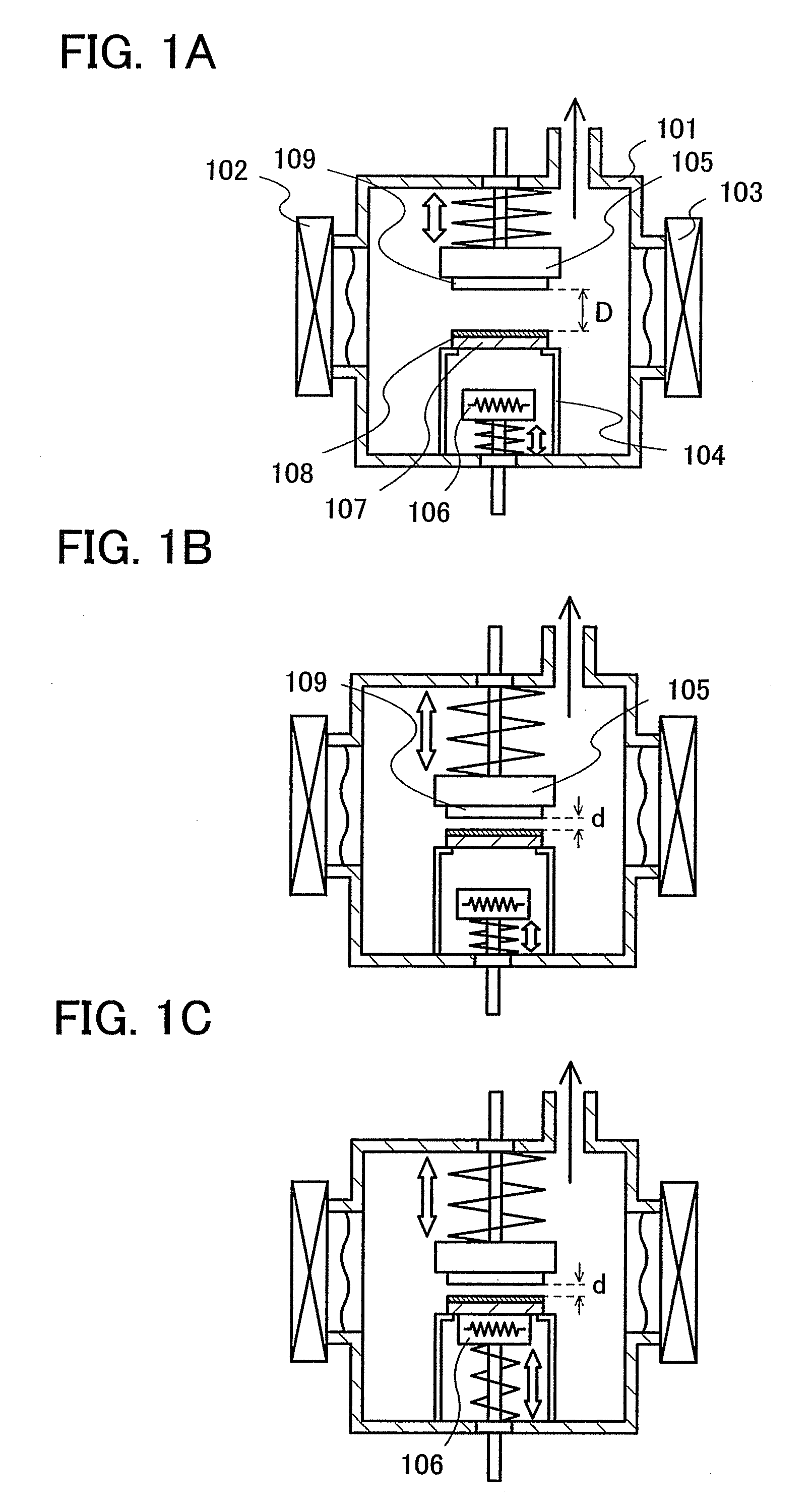
[0090]Although an example of a face-down film formation apparatus is described in Embodiment Mode 1, here, an example of a face-up film formation apparatus will be described using FIG. 3A.

[0091]In FIG. 3A, a film formation chamber 201 is a vacuum chamber and connected to other treatment chambers through a first gate valve 202 and a second gate valve 203. In the film formation chamber 201, at least, a supporting unit of a substrate on which a material layer 208 is to be formed (formation substrate), which is a first substrate supporting unit 205, a plate supporting unit which is a second substrate supporting unit 204, and a heater capable of vertical movement as a heat source 206 are included.

[0092]As the procedure of film formation, first, in the other film formation chamber, a material layer 208 is formed on a plate that is a second substrate 207. For a second substrate 207, there is no particular limitation on its shape as long as it has the area of more than or equal to that of t...

embodiment mode 3

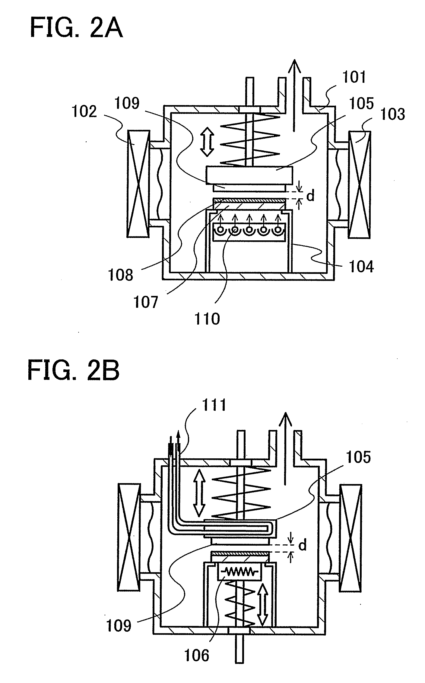
[0100]Although an example of the face-down film formation apparatus is described in Embodiment Mode 1, here, an example of a film formation apparatus employing vertical placement of a substrate will be illustrated in FIG. 4.

[0101]In FIG. 4, a film formation chamber 301 is a vacuum chamber. In the film formation chamber 301, at least, a plate supporting unit which is a first substrate supporting unit 304, a supporting unit of a substrate on which a material layer 308 is to be formed (formation substrate), which is a second substrate supporting mechanism 305, and a lamp 310 as a heat source are included.

[0102]Although not illustrated, the film formation chamber 301 is connected to a first transfer chamber to transfer the formation substrate while keeping vertical placement thereof and to a second transfer chamber to which a plate is transferred while keeping vertical placement thereof. It is to be noted that, in this specification, vertical placement of a substrate refers to placement...


PUM

PropertyMeasurementUnit
sizeaaaaaaaaaa
sizeaaaaaaaaaa
thicknessaaaaaaaaaa

Abstract

An object is to improve use efficiency of an evaporation material, to reduce manufacturing cost of a light-emitting device, and to reduce manufacturing time needed for a light-emitting device including a layer containing an organic compound. The pressure of a film formation chamber is reduced, a plate is rapidly heated by heat conduction or heat radiation by using a heat source, a material layer on a plate is vaporized in a short time to be evaporated to a substrate on which the material layer is to be formed (formation substrate), and then the material layer is formed on the formation substrate. The area of the plate that is heated rapidly is set to have the same size as the formation substrate and film formation on the formation substrate is completed by one application of heat.

Description

TECHNICAL FIELD[0001]The present invention relates to a film formation apparatus that is used for film formation of a material that can be formed on a substrate and a manufacturing apparatus including the film formation apparatus. The present invention further relates to a film formation method with the use of the film formation apparatus. Moreover, the present invention relates to a light-emitting device including, as a light-emitting layer, a layer containing an organic compound that is formed by the film formation apparatus, and a method for manufacturing the light-emitting device.BACKGROUND ART[0002]A light-emitting element containing an organic compound as a luminous body, which has features such as thinness, lightness, high-speed response, and DC drive at a low voltage, is expected to be applied to a next-generation flat panel display. In particular, a display device in which light-emitting elements are arranged in matrix is considered to have advantages in a wide viewing angl...

Claims


Application Information

Patent Timeline
Patent Type & Authority Applications(United States)
IPC IPC(8): B05D5/06B05C11/00B05C13/02
CPCC23C14/28C23C14/12B05C11/00C23C14/26H01L51/56C23C14/042C23C14/568H01L51/0081H10K85/324H10K71/00
Inventor IKEDA, HISAOAOYAMA, TOMOYAIBE, TAKAHIROHIRAKATA, YOSHIHARUYAMAZAKI, SHUNPEI
Owner SEMICON ENERGY LAB CO LTD
Why Eureka
Try Eureka