Thin-film solar cell and method of manufacturing the same

a solar cell and film technology, applied in the field of integrated thin film solar cell modules, can solve the problems of not being actively utilized, reducing the photoelectric conversion efficiency of the same, and not being exposed to light, so as to improve the photoelectric conversion efficiency, reduce the cost of manufacturing, and improve the effect of photoelectric conversion efficiency

Inactive Publication Date: 2008-10-30
LG ELECTRONICS INC
View PDF5 Cites 64 Cited by
  • Summary
  • Abstract
  • Description
  • Claims
  • Application Information

AI Technical Summary

Benefits of technology

[0017]The present invention has been suggested to solve the problems. It is an object of the present invention to provide a thin-film solar cell having a structure, which is capable of improving a photoelectric conversion effici

Problems solved by technology

A solar cell using monocrystalline bulk silicon, which is being commonly used at present, has a high photoelectric conversion efficiency, but the fact is that it is not being actively utilized due to high production and installation costs thereof.
However, the thin-film solar cell has problems such that the photoelectric conversion efficiency thereof is lower than that of a monocrystalline silicon solar cell and the efficiency is decreased when exposed to light.
For a solar cell using the other materials, in a case where the photoelectric conversion efficiency thereof is high, fabrication costs are increased and energy recovery period is extended, and in contrast, low fabrication costs and a short energy recovery period result in a low photoelectric conversion efficiency.
However, the solar cell structure on which the different double solar cell layers are stacked causes a problem such that the current of both the solar cell layers should be designed to be equal because both the solar cell layers are

Method used


Image

  • Thin-film solar cell and method of manufacturing the same
  • Thin-film solar cell and method of manufacturing the same
  • Thin-film solar cell and method of manufacturing the same

Examples


Embodiment Construction

[0057]Embodiments of the present invention will now be described hereafter with reference to the attached drawings. Reference numerals added to construction elements of each drawings use the same numerals within the range of the same construction elements, even though they are indicated in the other drawings, and the detailed description about well-known functions and structures, which are outside the subject matter of the present invention will be omitted.

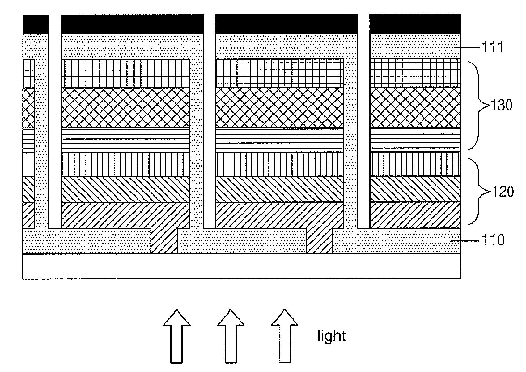
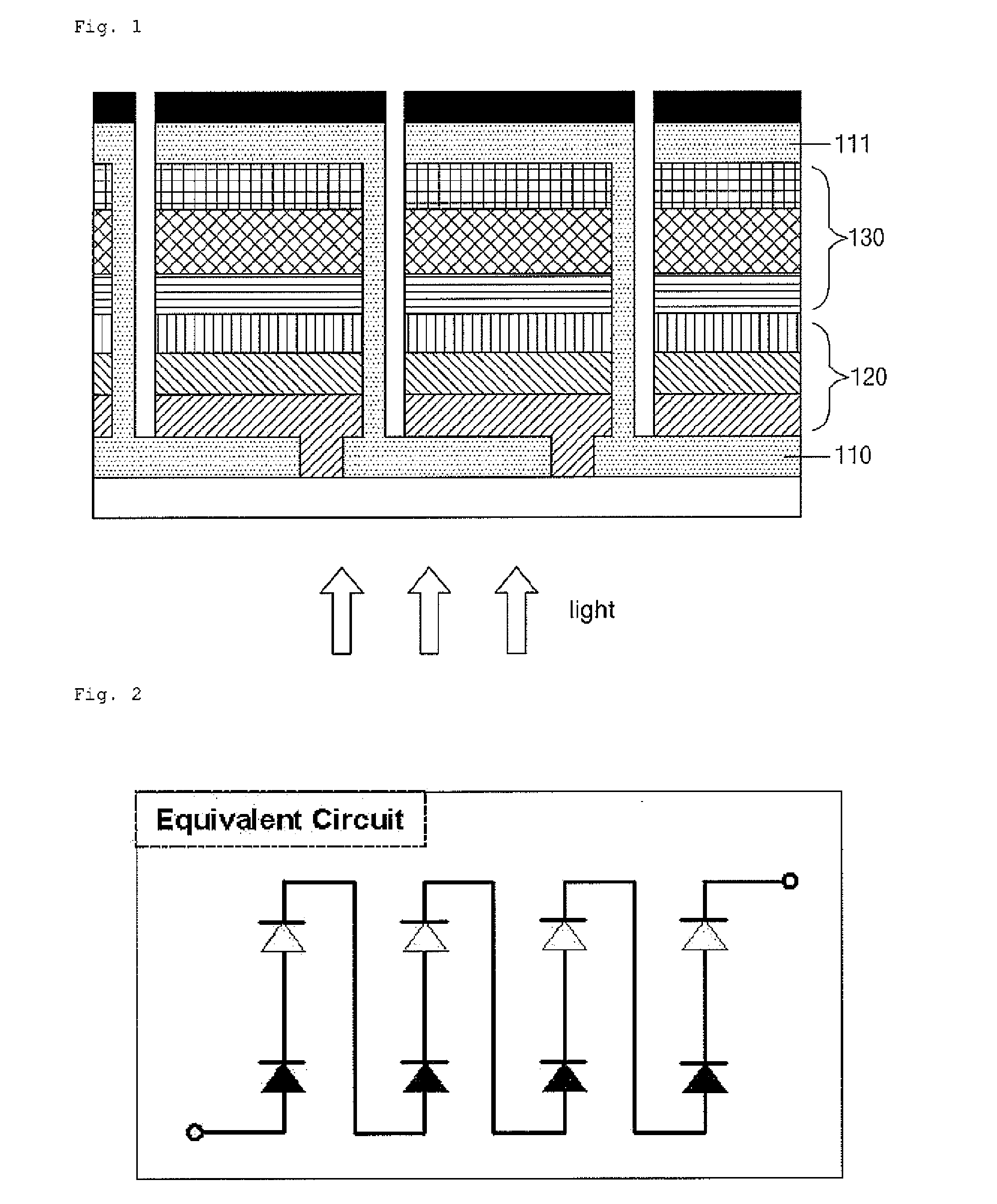
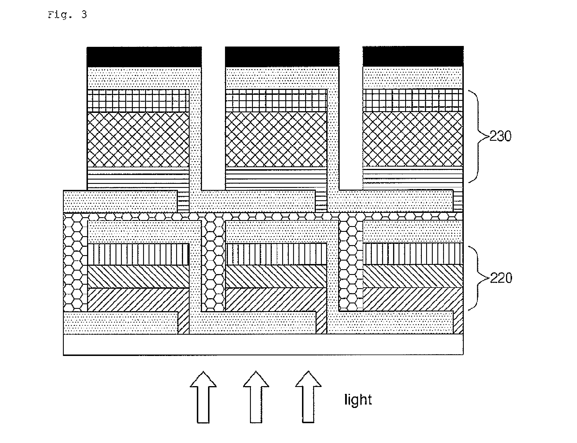
[0058]FIG. 5 is a sectional view illustrating a stack structure of the thin-film solar cell module according to the preferred embodiment of the present invention and FIG. 6 is a diode equivalent circuit of the thin-film solar cell module according to the preferred embodiment of the present invention.

[0059]In the preferred embodiment of the present invention, the thin-film solar cell is formed by stacking a substrate 300, the first solar cell layer 320, the second solar cell layer 330 and the back-side electrode layer 340; transpar...


PUM


Abstract

A thin-film solar cell of the present invention comprises a first solar cell layer that a plurality of unit cells including a photoelectric conversion layer are connected in series; a second solar cell layer that a plurality of unit cells including a photoelectric conversion layer are connected in series, which has band gap energy being different from the first solar cell layer and a threshold voltage being coincident with the first solar cell layer; and an electrode connector, which connects the first solar cell layer with the second solar cell layer in parallel.
The thin-film solar cell of the present invention provides a solar cell structure and a method of manufacturing the same, which is capable of increasing the efficiency by increasing the maximum output of the thin film solar cell formed of both the solar cell layers having the different characteristics.

Description

CROSS-REFERENCE TO RELATED APPLICATIONS[0001]This application claims the benefit of Korean Patent Application No. 10-2007-019097, filed on Feb. 26, 2007, in the Korean Intellectual Property Office, the disclosure of which is incorporated herein by reference.BACKGROUND[0002]1. Field of the Invention[0003]The present invention relates to an integrated thin-film solar cell module and a method of manufacturing the same, and more particularly, to a thin-film solar cell and a method of manufacturing the same, which are capable of improving a photoelectric conversion efficiency.[0004]2. Discussion of the Related Art[0005]The research in solar cells as next generation clean energy resources has been carried out for many years. Until recently, as materials for solar cells, materials of group IV such as monocrystalline silicon, polycrystalline silicon, amorphous silicon, amorphous SiC, amorphous SiN, amorphous SiCe and amorphous SiSn, and compound semiconductors of group III-V such as gallium...

Claims


Application Information

Patent Timeline
IPC IPC(8): H01L31/00H01L31/046H01L31/0463H01L31/05H01L31/06H01L31/076H01L31/078
CPCH01L31/02021H01L31/0392H01L31/076Y02E10/548H01L31/046H01L2924/0002H01L31/043H01L2924/00H01L31/03923H01L31/03925Y02E10/541Y02P70/50H01L31/06H01L31/18H01L31/0463
Inventor AHN, SEH-WONEO, YOUNG-JOOLEE, KWY-ROLEE, DON-HEELEE, HEON-MIN
Owner LG ELECTRONICS INC
Why Eureka
Try Eureka