
Method for manufacturing a crystalline silicon layer

a technology of crystalline silicon and manufacturing method, which is applied in the direction of photovoltaic energy generation, chemical vapor deposition coating, coating, etc., can solve the problems of low efficiency of devices such as traditional solar cells, negative effect of epitaxial growth on the quality of the layer, and serious technological challenges

Inactive Publication Date: 2008-10-30
INTERUNIVERSITAIR MICRO ELECTRONICS CENT (IMEC VZW)
View PDF10 Cites 22 Cited by
  • Summary
  • Abstract
  • Description
  • Claims
  • Application Information

AI Technical Summary

Problems solved by technology

However, most of these approaches have led to devices with much lower efficiency than traditional solar cells.
The presence of secondary crystallites and / or islands on the seed layer may have a negative effect on the quality of the layer that is grown epitaxially on top of the seed layer.
However, low temperature epitaxy on imperfect surfaces presents a serious technological challenge.
Standard low-cost glass cannot be used because it cannot withstand high temperatures.
Aluminum-induced crystallization on ceramic substrates however results in an average grain size that is low (e.g., about 1 to 2 micron), and a high density of islands.
While the above-described methods of MIC have produced crystalline silicon on foreign substrates, these techniques have not produced silicon layers with high enough crystalline quality for many uses, such as for use in solar cells.

Method used


Image

  • Method for manufacturing a crystalline silicon layer
  • Method for manufacturing a crystalline silicon layer
  • Method for manufacturing a crystalline silicon layer

Examples


example 1

AIC on Bare Ceramic Substrate 1a (Comparative Example)

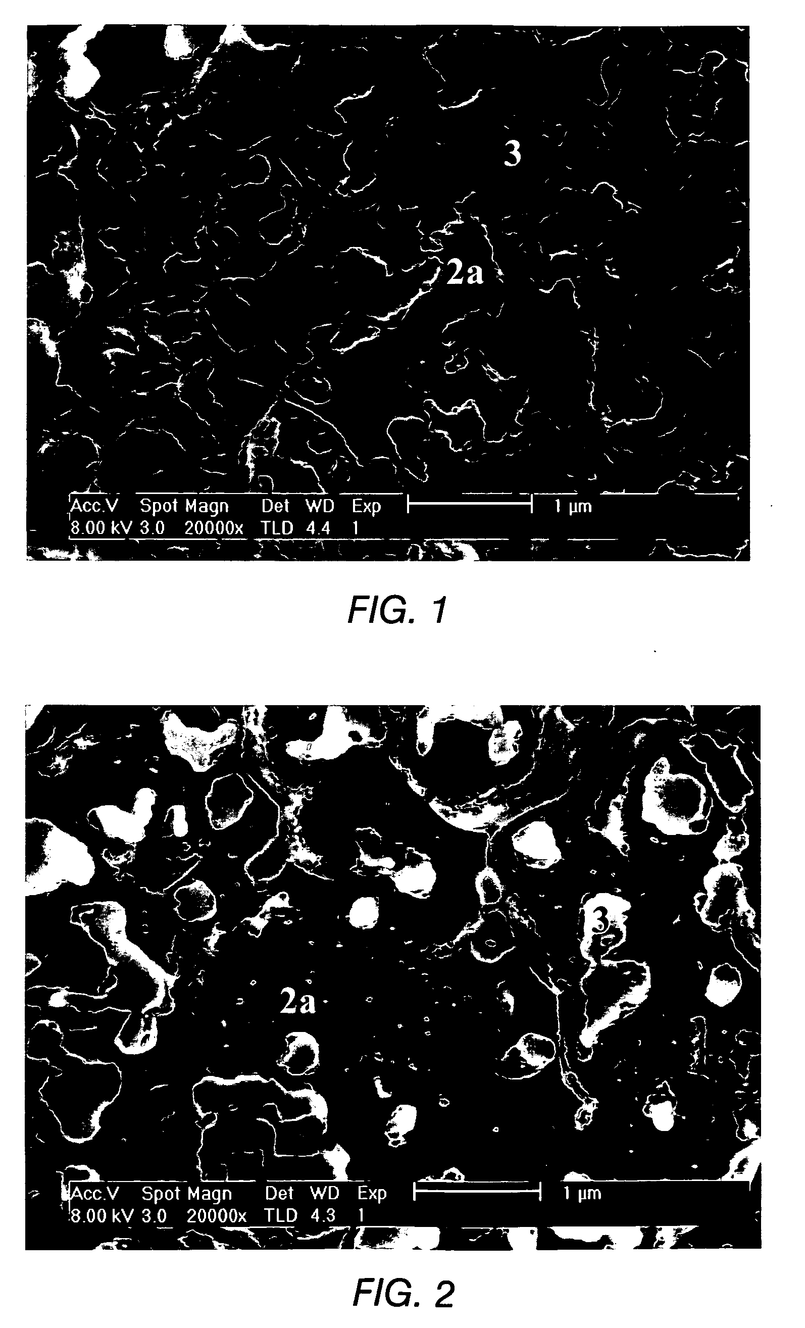
[0096]The morphology of a typical sample obtained with the procedure described above can be seen in the SEM picture in FIG. 1. The AIC seed layer 2a as such is not clearly visible in this picture. The reason is that the layer 2a is covered by numerous ‘islands’3, the secondary crystallites formed within the top layer during the AIC process. Close observation with SEM and TEM analysis reveals that the grain size in the AIC seed layer 2a is around 1-2 μm. This grain size is substantially lower than reported results on glass. There appears to be much more nucleation taking place when the AIC is done on a ceramic substrate 1a, both in the bottom layer (leading to a small grain size) and in the top layer (leading to a high density of islands).

example 2

Intermediate Layer Applied in Order to Reduce the Microroughness

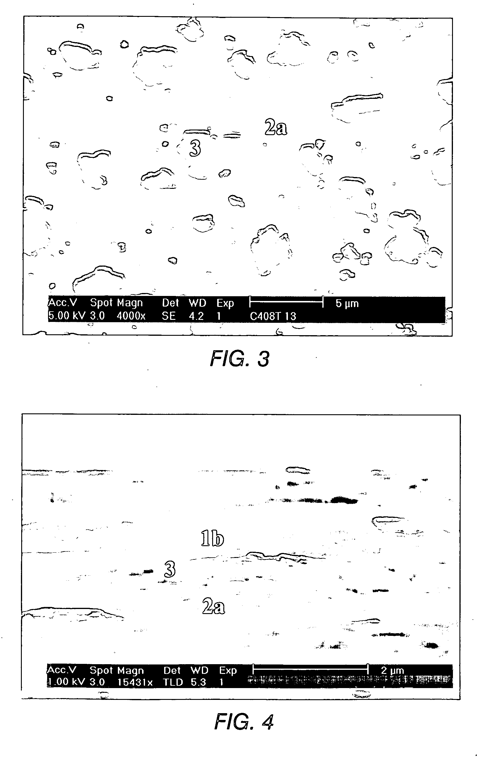
[0097]An intermediate silicon oxide layer was introduced between the substrate 1a and the AIC layers. Two different types of oxide were used. One type was a pyrolithic oxide (‘pyrox’) deposited by the decomposition of silane at atmospheric pressure and 400° C. The second type was a spin-on flowable oxide (FOx-23 from Dow Corning), cured at 400° C. Pyrox was densified at 950° C. and the spin-on flowable oxide at 900° C. before the deposition of the AIC stack. SEM pictures of these samples are shown in FIG. 2 and FIG. 3, respectively. The density of islands 3 decreased significantly compared to Example 1, by about a factor two for the intermediate pyrox layer (FIG. 2), and another factor 2 for the spin-on oxide layer (FIG. 3). The appearance of the latter samples is however completely different. Because there are much less islands 3 in the case of the spin-on oxide, the structure of the main AIC seeding layer 2a is clearl...

example 3

Epitaxial Silicon Deposition

[0099]After removal of the metal layer obtained on top of the stack at the end of the MIC process, e.g. an Al layer in case of an AIC process, high temperature CVD was used to deposit an epitaxial layer on top of the seed layer 2a, an established technique common in the microelectronics processing. AIC seed layers 2a were prepared on spin-on flowable oxide 1b covering 5×5 cm2 alumina samples 1a following the procedure described above. The conditions were such that the AIC layers 2a covered the complete surface. No attempt was made at removing the islands 3 from the seed layer 2a. Si layers 2b were deposited on these samples in a commercial single-wafer epitaxial reactor (Epsilon ASM) with trichlorosilane diluted in H2, at atmospheric pressure and at a temperature of 1130° C. The deposition rate was 1.4 μm / min. In situ doping with B was done by adding diborane to the gas flow, so as to form double layers with a 0.5-3 μm thick p+ region (˜1019 cm−3) and a 0...


PUM

PropertyMeasurementUnit
temperatureaaaaaaaaaa
grain sizesaaaaaaaaaa
grain sizeaaaaaaaaaa

Abstract

A method of forming a crystalline silicon layer on a microrough face of a substrate by reducing the microroughness of the face and then performing a metal induced crystallization process on the face is disclosed. The method further comprises, after metal induced crystallization and before removing the metal layer, removing silicon islands using the metal layer as a mask.

Description

CROSS-REFERENCE TO RELATED APPLICATIONS[0001]This application is a continuation-in-part of U.S. application Ser. No. 11 / 146,564, filed Jun. 7, 2005, which claims priority under 35 U.S.C. § 119(e) to U.S. Provisional Appl. No. 60 / 577,556, filed Jun. 7, 2004. This application also claims priority under 35 U.S.C. § 119(e) to U.S. Provisional Appl. No. 60 / 917,578, filed May 11, 2007. The disclosures of each of the foregoing applications are hereby incorporated by reference in their entireties and are hereby made a portion of this application.FIELD OF THE INVENTION[0002]Methods for manufacturing crystalline silicon layers on a substrate are provided, including a Metal Induced Crystallization process. The application of such methods in the manufacturing process of electronic devices such as solar cells is also provided.BACKGROUND OF THE INVENTION[0003]Thin-film crystalline Si solar cells on cheap foreign substrates are a promising alternative to traditional bulk crystalline silicon solar ...

Claims


Application Information

Patent Timeline
Patent Type & Authority Applications(United States)
IPC IPC(8): H01L21/20
CPCH01L21/02422H01L21/02488H01L21/02532H01L21/02672H01L31/03921H01L31/1872Y02E10/50Y02P70/50
Inventor VAN GESTEL, DRIES
Owner INTERUNIVERSITAIR MICRO ELECTRONICS CENT (IMEC VZW)
Learn More