Method for preparing polycrystalline silicon film by carrying out induced crystallization on amorphous silicon film by using metallic copper under low temperature

A technology of amorphous silicon thin film and polycrystalline silicon thin film, which is applied in metal material coating technology, semiconductor devices, gaseous chemical plating, etc., can solve problems such as unsuitability, high material defect density, high grain boundary density, etc., and achieve compatibility Enhanced effect

Inactive Publication Date: 2012-10-03
SHANGHAI UNIV
View PDF6 Cites 8 Cited by
  • Summary
  • Abstract
  • Description
  • Claims
  • Application Information

AI Technical Summary

Problems solved by technology

Films with different grain sizes can be prepared by controlling the time and temperature of the three stages of heating up, stabilizing, and cooling. The boundary density is large, the material defect density is high, and it is a high-temperature annealing method, which is not suitable for preparing polysilicon with glass as a substrate.

Method used


Image

  • Method for preparing polycrystalline silicon film by carrying out induced crystallization on amorphous silicon film by using metallic copper under low temperature
  • Method for preparing polycrystalline silicon film by carrying out induced crystallization on amorphous silicon film by using metallic copper under low temperature

Examples


Embodiment

[0027] The process and steps in the embodiment of the present invention are as follows:

[0028] (1) Cut a piece of ordinary Corning glass into 1cm×1cm size, clean the surface dirt with Triton solvent, then ultrasonically clean it in acetone, absolute ethanol and deionized water for 15 minutes, and dry it with nitrogen;

[0029] (2) Deposit a layer of amorphous silicon (a-Si:H) film on the cleaned substrate by plasma-enhanced chemical deposition (PECVD), with a thickness of about 300nm. The substrate temperature during deposition is 250°C, and the deposition pressure is for 10 -5 Pa, gas glow pressure range 50Pa-200Pa, RF power supply 13.56MHz, gas source is silane with a purity of 99.999% (SiH 4 ), the purity of hydrogen used as dilute silane is 5N (99.999%), where H 2 The proportion of mixed gas is about 2%;

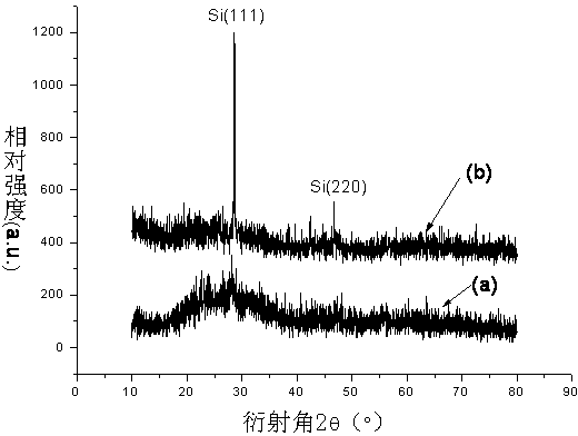
[0030] (3) Place the grown amorphous silicon thin film sample in an oxygen chamber for 5 h at room temperature, put it in a magnetron sputtering vacuum chamber, and...


PUM

PropertyMeasurementUnit
thicknessaaaaaaaaaa
particle sizeaaaaaaaaaa

Abstract

The invention relates to a preparation method of a polycrystalline silicon film, in particular to a method for preparing a polycrystalline silicon film by carrying out induced crystallization on an amorphous silicon film by cycle annealing under low temperature by using catalytic action of metallic copper. The main technical scheme of the invention is as follows: the method comprises the following steps of: growing a substrate / amorphous silicon / silicon dioxide / copper film structure on a glass substrate, then carrying out cycle annealing, putting a sample in corrosive liquid for corroding after first annealing is finished, and carrying out cycle annealing and corroding again, and drying the sample with nitrogen; and finally preparing the polycrystalline silicon film prepared by induced crystallization by copper, wherein the grain size is about 50-200nm. The method disclosed by the invention can ease the problem of serious metal pollution in the traditional MIC (Metal Induced Crystallization) technology and is suitable for the field of thin film field effect transistors and thin-film solar cells.

Description

technical field [0001] The invention relates to a preparation method of a polysilicon thin film, specifically a method for inducing the crystallization of an amorphous silicon thin film into a polysilicon thin film at a low temperature by utilizing the catalysis of metal copper. Background technique [0002] At present, the methods for preparing polysilicon thin films mainly include: low pressure chemical vapor deposition (LPCVD), solid phase crystallization (SPC), excimer laser induced crystallization (ELA), rapid thermal annealing crystallization (RTA), etc. [0003] The polysilicon film prepared by LPCVD method is dense and uniform, and can be produced in a large area, but when prepared by this method, the required substrate temperature is high and the deposition speed is slow, and cheap glass cannot be used as the substrate. The most important thing is that the polysilicon film deposited by this method has smaller particles, resulting in more grain boundaries and more de...

Claims


Application Information

Patent Timeline
Patent Type & Authority Applications(China)
IPC IPC(8): H01L31/20C23C16/44
CPCY02P70/50
Inventor 史伟民周平生周平华李杰瞿晓雷廖阳钱隽李季戎张月璐许月阳
Owner SHANGHAI UNIV
Why Eureka
Try Eureka