Multi-chip semiconductor device having leads and method for fabricating the same

a semiconductor device and multi-chip technology, applied in the field of semiconductor devices, can solve the problems of affecting the reliability of the interface between the substrate and the die pad of the lead frame, the inability of conventional lead frame type semiconductor packages to provide sufficient electrical connection among a plurality of chips, and the proneness of the semiconductor package to crack, etc., to achieve the effect of increasing the heat dissipation of the multi-chip semiconductor device, simplifying the fabrication process, and reinforcing the connection between the lead

Inactive Publication Date: 2008-11-20
SILICONWARE PRECISION IND CO LTD
View PDF8 Cites 5 Cited by
  • Summary
  • Abstract
  • Description
  • Claims
  • Application Information

AI Technical Summary

Benefits of technology

[0019]Moreover, a ring-shaped reinforcing element can be disposed on the leads to reinforce the connection between the leads and the substrate of the package unit. Alternatively, a heat dissipating element having a concave portion can be disposed on the leads and the top of the encapsulant, thereby increasing heat dissipation of the multi-chip semiconductor device and reinforcing the connection among the leads and the substrate. Furthermore, a plurality of solder balls can be mounted on a surface opposed to the surface where the encapsulant is formed, of the package unit, to provide an additional path for signal transmission and heat conduction. In addition, taken electrical requirements into consideration, a plurality of exposed solder pads with different electrical properties are formed on a surface opposed to the surface where the encapsulant is formed, so as to allow the multi-chip semiconductor device to be electrically connected to the when being mounted to an external device such as a printed circuit board (PCB). Therefore, by the multi-chip semiconductor device having leads and the method for fabricating the same, of the present invention, a substrate having a plurality of connection pads disposed on a surface thereof is provided, a plurality of semiconductor chips mounted on and electrically connected to the surface of the substrate, an encapsulant is formed to encapsulates the semiconductor chips and expose the connection pads to form a package unit, subsequently the exposed connection pads in the package unit are physically and electrically connected to the leads of the lead frame, to obtain a semiconductor device having a MCM and leads. The multi-chip semiconductor device of the present invention is fabricated by performing a simplified fabrication processes and is cost-effective. Moreover, unlike prior arts, the present invention can avoid poor reliability caused by a stress induced by several types of materials in a semiconductor package in which a substrate and leads are integrated, moisture absorption by an encapsulated substrate, and cracks developed as a result of moisture absorption by the substrate.

Problems solved by technology

However, conventional lead frame type semiconductor packages as single layer structures cannot provide sufficient electrical connection among a plurality of chips mounted on a single-layered lead frame.
Nevertheless, in the above semiconductor package, reliability of interface between the substrate and the die pad of the lead frame is often adversely affected by a stress induced by different materials.
Moreover, as the substrate material inside the semiconductor package readily absorbs moisture, the semiconductor package is prone to developing cracks.
Additionally, disposal of a substrate on a die pad with a limited area cannot allow integration of multiple chips in a semiconductor package at the same time, thereby limiting uses of this type of multi-layer lead frame having a multi-layered structure.
However, as the lead frame is integrated to the inside of the substrate, fabrication of the semiconductor package is difficult.
Also, since the leads (which are made of metal) are disposed on the inside the resin substrate (which are made of resin), stress induced by different interfaces can result in poor reliability of the package.
Therefore, the problem to be solved herein is to provide a multi-chip semiconductor device and method for fabricating the same, which can integrate a plurality of semiconductor chips therein and solve problems such as stress induced by several types of materials, moisture absorption by an encapsulated substrate, and poor reliability caused by encapsulated leads.

Method used


Image

  • Multi-chip semiconductor device having leads and method for fabricating the same
  • Multi-chip semiconductor device having leads and method for fabricating the same
  • Multi-chip semiconductor device having leads and method for fabricating the same

Examples


first embodiment

[0029]FIGS. 3A to 3E are schematic diagrams showing a multi-chip semiconductor device having leads and a method for fabricating the same according to a first embodiment of the present invention. In this embodiment, a batch-type method is employed to fabricate the multi-chip semiconductor device having leads. It should be understood that the multi-chip semiconductor device having leads of the present invention can also be fabricated in a singular-type manner under suitable fabrication conditions.

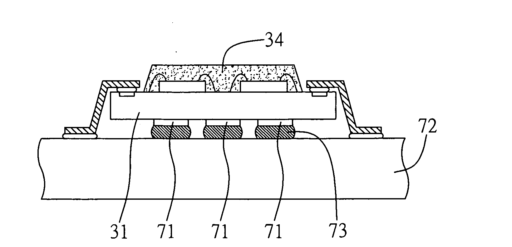
[0030]Referring to FIG. 3A, a substrate module plate 310 having a plurality of substrates 31 is provided. A plurality of connection pads 311 are disposed on a surface of each of the substrates 31, for mounting a plurality of semiconductor chips 32 on each of the substrates 31, wherein the connection pads 311 are disposed on edges of the substrates 31. The semiconductor chips 32 can be electrically connected to the substrates 31, via a plurality of bonding wires 33 or by a flip-chip process.

[0...

second embodiment

[0037]FIGS. 4A and 4B are schematic diagrams showing a multi-chip semiconductor device having leads and a method for fabricating the same according to a second embodiment of the present invention, wherein elements that are same as or similar to the above-described elements are denoted by the same reference numerals to facilitate illustration and understanding.

[0038]The major difference between the present embodiment and the first embodiment is that after the connections pads exposed from the encapsulant of the package unit is electrically connected to the leads of the lead frame, a ring-shaped reinforcing element 41 is disposed on the leads 351 via a non-conductive medium 42, and the encapsulant 34 of the package unit is accommodated in a ring-shaped opening 410 of the reinforcing element 41, thereby reinforcing the connection between the leads 351 and the substrate 31 of the package unit.

third embodiment

[0039]FIG. 5 is a schematic diagram showing a multi-chip semiconductor device having leads and a method for fabricating the same according to a third embodiment of the present invention, wherein elements that are same as or similar to the above-described elements are denoted by the same reference numerals to facilitate illustration and understanding.

[0040]The major difference between the present embodiment and the previous embodiments is that after the connections pads exposed from the encapsulant of the package unit is electrically connected to the leads of the lead frame, a heat dissipating element 51 having a concave portion 510 is disposed on the leads 351 via a non-conductive medium 52. The concave portion 510 and is mounted on the encapsulant 34 via a thermal conductive medium 53 therebetween (i.e., the thermal conductive medium 53 is in contact with the top of the concave portion 510 and the top of the encapsulant 34), thereby increasing heat dissipation of the multi-chip sem...


PUM


Abstract

The present invention proposes a multi-chip semiconductor device having leads and a method for fabricating the same. The method includes the steps of: providing a substrate having a plurality of connection pads disposed on a surface thereof; mounting a plurality of semiconductor chips on the surface of the substrate, and electrically connecting the semiconductor chips to the surface of the substrate; forming an encapsulant on the substrate to encapsulate the semiconductor chips and expose the connection pads to form a package unit; and providing a lead frame having a plurality of leads, and electrically connecting the connection pads exposed from the package unit to the leads of the lead frame to form a multi-chip semiconductor device having leads, thereby forming a multi-chip semiconductor device having leads. By the multi-chip semiconductor device and the method for fabricating the same as proposed in the present invention, problems like poor reliability caused by stress induced by several types of materials in a semiconductor package into which a substrate and leads are integrated, moisture absorption by an encapsulated substrate, and cracks developed as a result of moisture absorption by the substrate can be avoided.

Description

BACKGROUND OF THE INVENTION[0001]1. Field of the Invention[0002]The present invention relates to semiconductor devices and methods for fabricating the same, and more particularly, to a multi-chip semiconductor device having leads and a method for fabricating the same.[0003]2. Description of Related Art[0004]A conventional lead frame type semiconductor package, such as a quad flat package (QFP), is fabricated by attaching a chip to a lead frame having a die pad and a plurality of leads, electrically connecting a plurality of solder pads disposed on an upper surface of the chip to the corresponding leads via a plurality of bonding wires, and encapsulating the chip and the bonding wires by an encapsulant to form a lead frame type semiconductor package. Please refer to U.S. Pat. Nos. 5,874,773, 6,696,750, 6,902,102 and 7,057,293, for information on related techniques.[0005]Moreover, in order to meet the increasing demand for miniaturization and high operation speed of electronic product...

Claims


Application Information

Patent Timeline
Patent Type & Authority Applications(United States)
IPC IPC(8): H01L21/58H01L23/495
CPCH01L23/3121H01L23/49811H01L23/49816H01L23/49861H01L24/81H01L24/85H01L24/97H01L25/0655H01L2224/48091H01L2224/48247H01L2224/81801H01L2224/97H01L2924/01082H01L2924/15311H05K1/141H05K3/3421H05K3/3436H05K2201/1034H05K2201/10659H01L2924/00014H01L2224/85H01L24/48H01L2924/01033H01L2924/181H01L2924/00012H01L2224/45099H01L2224/45015H01L2924/207
Inventor LIU, CHUNG-LUNCHANG, CHIN-HUANGHUANG, CHIEN-PINGCHAN, CHANG-YUEHHUANG, CHIH-MING
Owner SILICONWARE PRECISION IND CO LTD
Why Eureka
Try Eureka