Printed circuit board provided with heat circulating medium and method for manufacturing the same

a technology of printed circuit boards and heat circulating medium, which is applied in the direction of stacked and attached pcbs, transportation and packaging, and other domestic objects, can solve problems such as system failure, circuitry malfunction, and hot spots generated, and achieve the effect of preventing temperature ris

Active Publication Date: 2008-11-20
SK HYNIX INC
View PDF2 Cites 19 Cited by
  • Summary
  • Abstract
  • Description
  • Claims
  • Application Information

AI Technical Summary

Benefits of technology

[0009]Embodiments of the present invention are directed to a PCB provided with a heat circulation medium capable of preventing temperature rising, and a method for manufacturing the same.
[0010]Further, embodiments of the present invention are directed to a PCB, capable of preventing temperature rising and thus adapted to realize a high performance electronic machine, and a method for manufacturing the same.

Problems solved by technology

However, in a conventional PCB as shown in FIG. 1, hot spots are generated due to the differences in the level of power consumption between parts such as the semiconductor packages that are mounted on the PCB to construct a memory module, a mother board for a PC, a graphic card for PC, and the like.
Further, the circuitry malfunction may be caused by the rising PCB temperature due to the diffusion resistance resulting from the generation of hot spots.
Thus, the rise of PCB temperature due to localized hot spots may lead to the system failure or poor operation of the system.
Particularly, the thermal conductivity of an insulation layer in a conventional PCB is generally low.
As the conventional PCBs rely on the conductive layer that is relatively smaller in portion than the insulation layer for heat dissipation, the issue of potential system failure due to the rising temperature of the PCB will be more problematic as even greater number of semiconductor packages are mounted on a PCB in a high performance electronic machine.

Method used


Image

  • Printed circuit board provided with heat circulating medium and method for manufacturing the same
  • Printed circuit board provided with heat circulating medium and method for manufacturing the same
  • Printed circuit board provided with heat circulating medium and method for manufacturing the same

Examples


Embodiment Construction

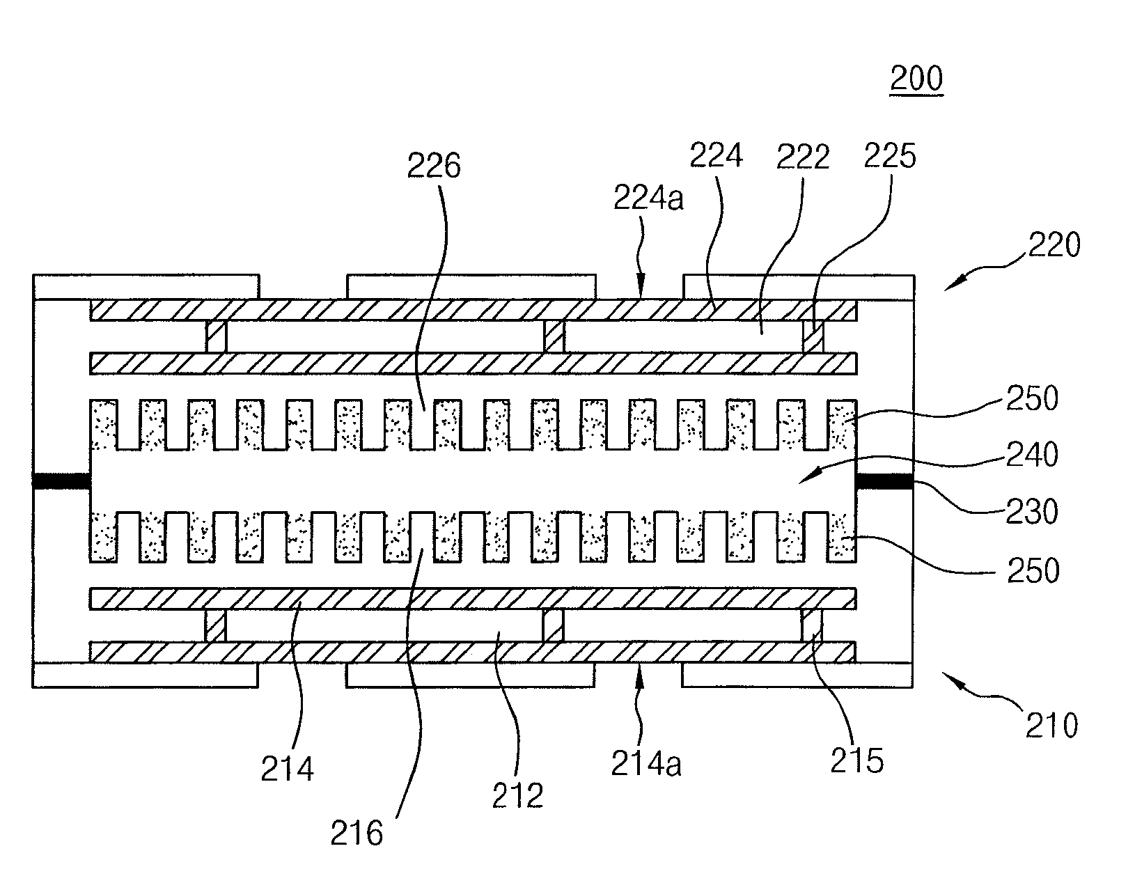
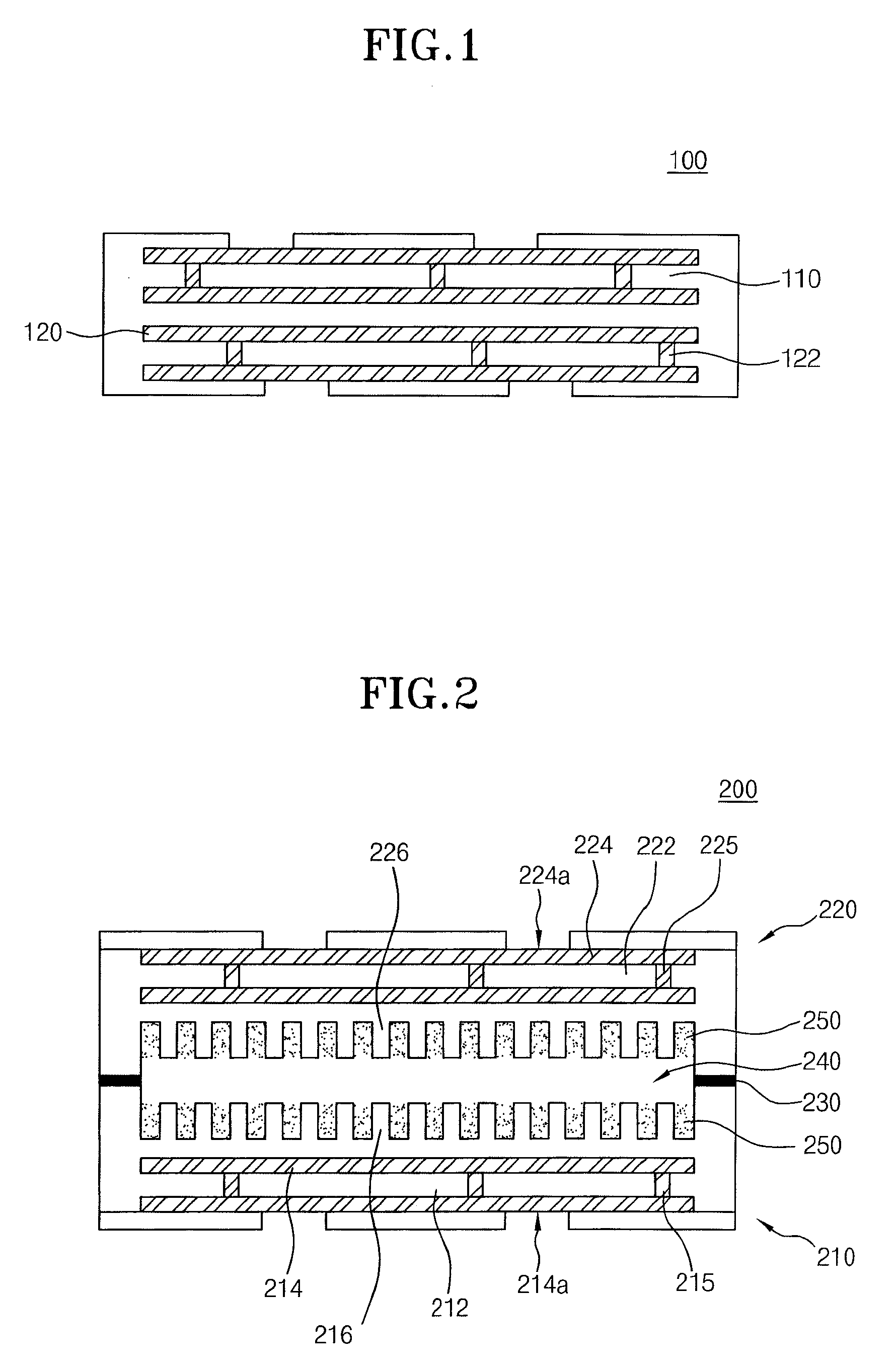
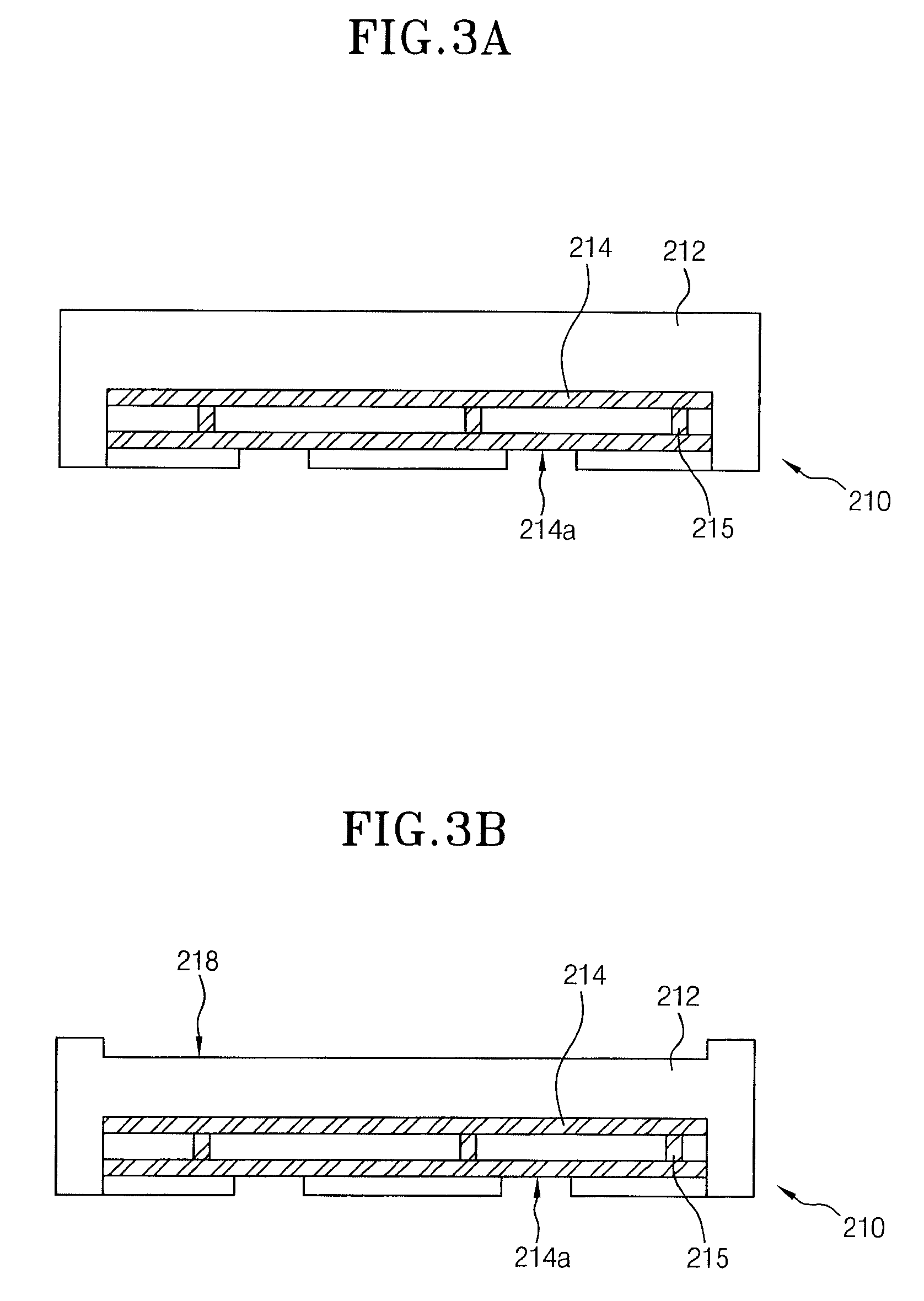
[0025]A preferred embodiment of the present invention is directed to a PCB having an upper plate provided with an internal circuit wiring and a lower plate provided with an internal circuit wiring, in which recessed parts are formed on each surface of the upper plate and the lower plate such that the surfaces of the upper and lower plates provided with the recessed parts are adhered to each other so that a heat circulation medium (e.g., a fluid) is injected into the cavities formed by the recessed parts.

[0026]Accordingly, the temperature rising in the localized sections of the PCB is prevented by spreading the heat to the entire PCB by circulating the injected heat circulation medium undergoing the cycles of vaporization, movement, condensation and return, thereby lowering the localized high temperatures found on the PCB. Therefore, the PCB made in accordance with an embodiment of the present invention has an enhanced heat radiation property for effective lowering of higher temperat...


PUM

PropertyMeasurementUnit
widthaaaaaaaaaa
heightaaaaaaaaaa
adhesionaaaaaaaaaa

Abstract

A printed circuit board includes a lower plate provided with an internal circuit wiring and having a recessed part at a surface thereof and a plurality of projection patterns at a lower surface of the recessed part; an upper plate having the same structure of the lower plate and adhered to the lower plate so that surfaces formed with the recessed part are opposite to each other; a heat circulation medium injected into an internal space formed by the recessed parts of the lower and upper plates.

Description

CROSS-REFERENCE TO RELATED APPLICATIONS[0001]The present application claims priority to Korean patent application number 10-2007-0047017 filed on May 15, 2007, which is incorporated herein by reference in its entirety.BACKGROUND OF THE INVENTION[0002]The present invention relates to a printed circuit board, and more particularly to a printed circuit board provided with a heat circulating medium, and a method for manufacturing the same.[0003]The recent trend in the electronic industry for mounting techniques utilizes printed circuit boards (PCBs) for high density and high accuracy mounting of mounting parts employed to achieve a miniaturization and a high performance of an electronic machine. Particularly, high density PCBs capable of mounting more memory parts such as semiconductor packages are gaining attention as the chip size package (CSP) technique such as a ball grid array (BGA) and a tape carrier package (TCP) is developed. Therefore, a PCB which allows a high density mounting...

Claims


Application Information

Patent Timeline
Patent Type & Authority Applications(United States)
IPC IPC(8): B32B3/00B32B38/06
CPCB32B38/0012B32B2038/0016B32B2309/10B32B2457/08H05K1/0203Y10T428/24612H05K3/4623H05K2201/043H05K2201/064H05K2203/061Y10T29/49156H05K1/0272H05K1/02H05K7/20
Inventor SON, JAE HYUN
Owner SK HYNIX INC
Why Eureka
Try Eureka