Extensions of Self-Assembled Structures to Increased Dimensions via a "Bootstrap" Self-Templating Method

a self-templating and self-assembled technology, applied in the field of nanoscale array fabrication methods, can solve the problems of limiting the dimensions of structures produced by selective etching and removal of polymer domains of films, the necessity of casting only very thin films, and the inability to meet the requirements of critical dimensions of desired features,

Active Publication Date: 2008-11-20
MICRON TECH INC
View PDF99 Cites 78 Cited by
  • Summary
  • Abstract
  • Description
  • Claims
  • Application Information

AI Technical Summary

Problems solved by technology

Conventional optical lithographic processing methods are not able to accommodate fabrication of structures and features much below the 100 nm level.
While the self-assembly of diblock copolymers of tightly controlled composition and polydispersity has been demonstrated as a method of preparing a variety of nanoscale, sub-lithographic structures, the necessity of casting only very thin films limits the dimensions of the structures, particularly in the z-axis direction (i.e., perpendicular to the substrate surface).
Openings produced by selective etching and removal of polymer domains of the films may not achieve the required aspect ratio for critical dimensions of desired features.

Method used


Image

  • Extensions of Self-Assembled Structures to Increased Dimensions via a "Bootstrap" Self-Templating Method
  • Extensions of Self-Assembled Structures to Increased Dimensions via a "Bootstrap" Self-Templating Method
  • Extensions of Self-Assembled Structures to Increased Dimensions via a "Bootstrap" Self-Templating Method

Examples


Embodiment Construction

[0025]The following description with reference to the drawings provides illustrative examples of devices and methods according to embodiments of the invention. Such description is for illustrative purposes only and not for purposes of limiting the same.

[0026]In the context of the current application, the term “semiconductor substrate” or “semiconductive substrate” or “semiconductive wafer fragment” or “wafer fragment” or “wafer” will be understood to mean any construction comprising semiconductor material, including but not limited to bulk semiconductive materials such as a semiconductor wafer (either alone or in assemblies comprising other materials thereon), and semiconductive material layers (either alone or in assemblies comprising other materials). The term “substrate” refers to any supporting structure including, but not limited to, the semiconductive substrates, wafer fragments or wafers described above.

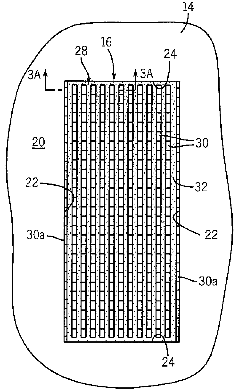
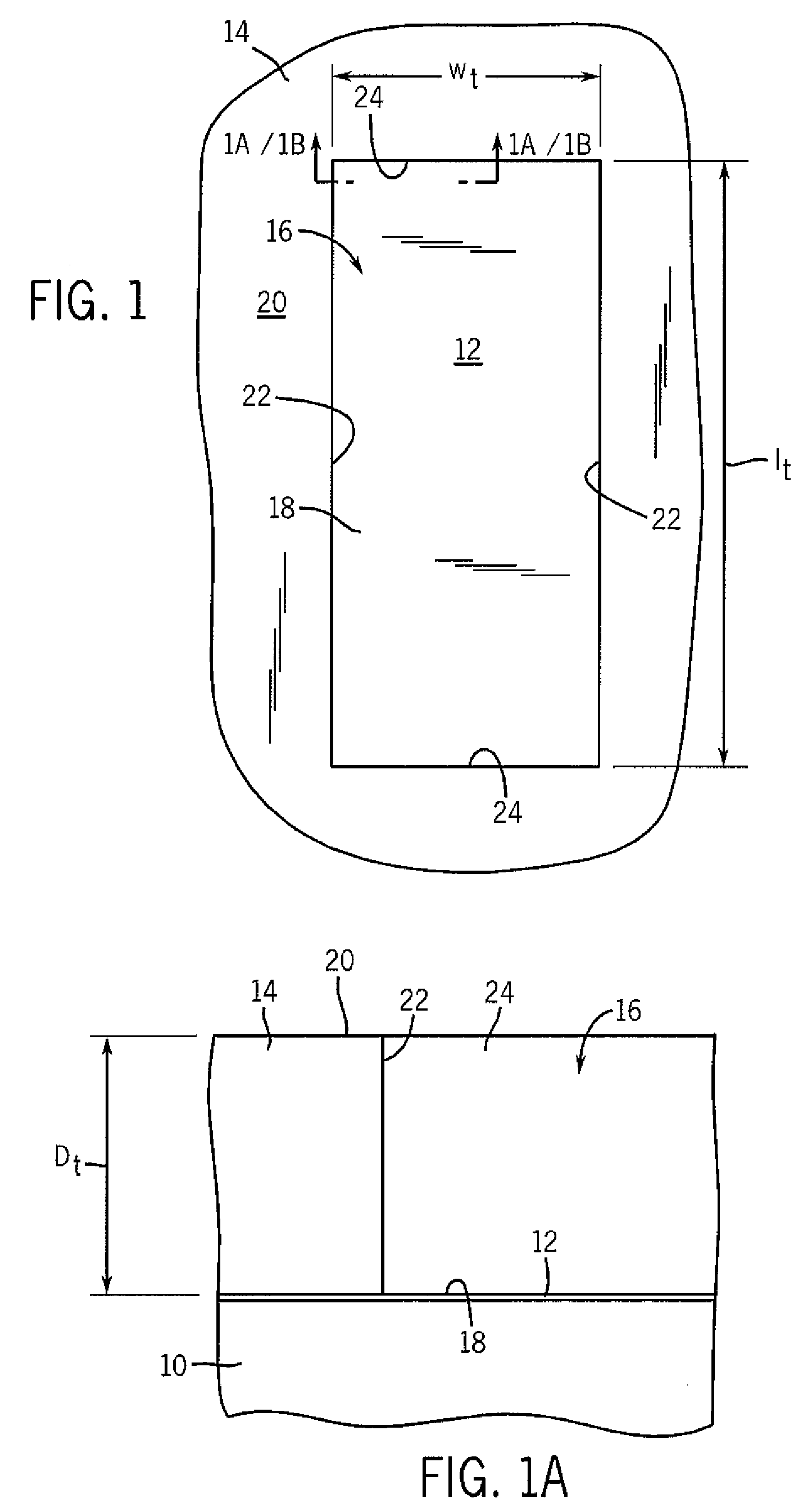
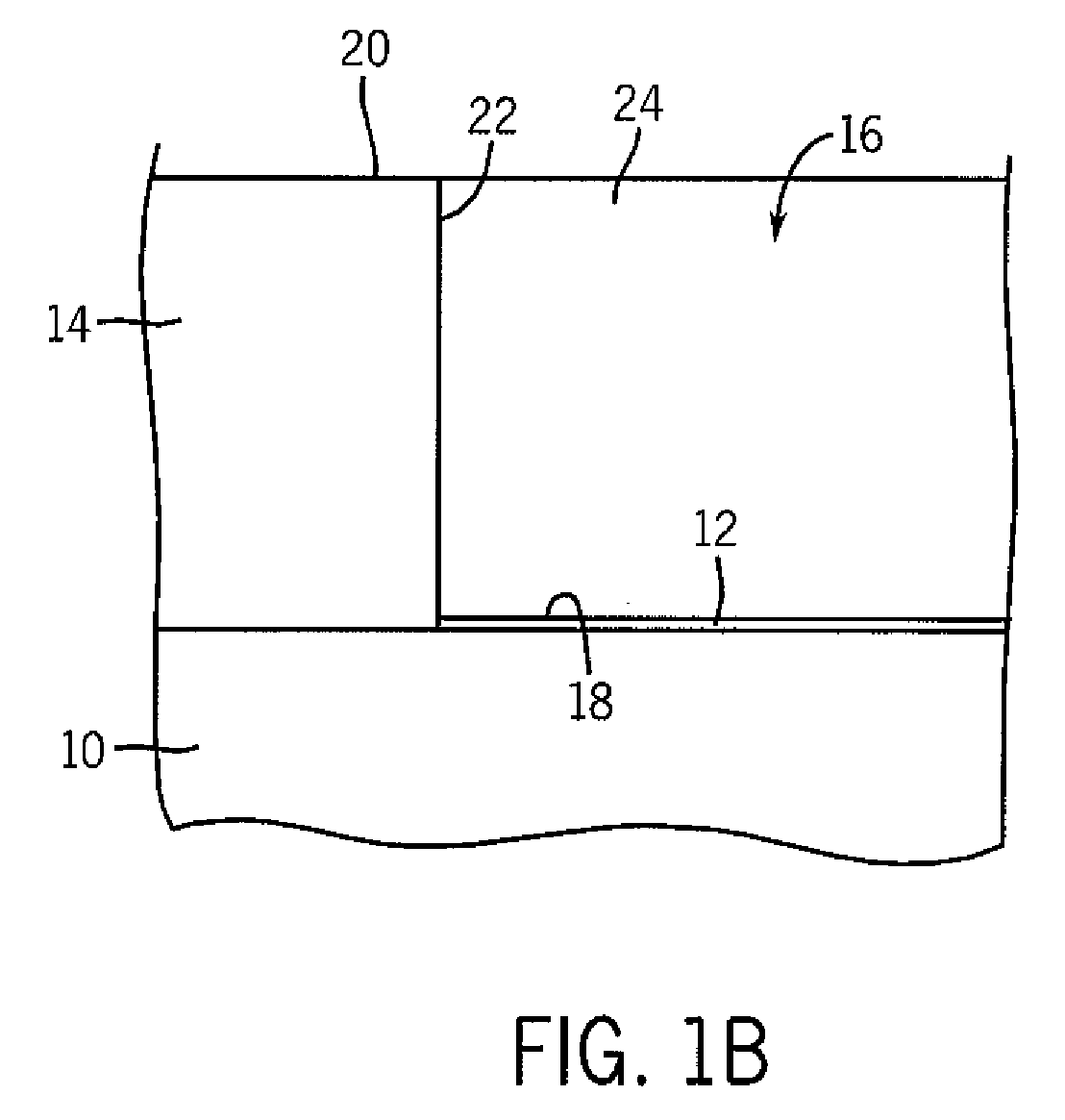
[0027]Lo is the inherent pitch (bulk period or repeat unit) of structures...


PUM

PropertyMeasurementUnit
widthaaaaaaaaaa
thickaaaaaaaaaa
thickaaaaaaaaaa

Abstract

Methods for fabricating sublithographic, nanoscale arrays of openings and linear microchannels utilizing self-assembling block copolymers, and films and devices formed from these methods are provided. Embodiments of the invention use a self-templating or multilayer approach to induce ordering of a self-assembling block copolymer film to an underlying base film to produce a multilayered film having an ordered array of nanostructures that can be removed to provide openings in the film which, in some embodiments, can be used as a template or mask to etch openings in an underlying material layer.

Description

TECHNICAL FIELD[0001]Embodiments of the invention relate to methods of fabricating nanoscale arrays of micro-vias, microchannels and microstructures by use of thin films of self-assembling block copolymers, and devices resulting from those methods.BACKGROUND OF THE INVENTION[0002]As the development of nanoscale mechanical, electrical, chemical and biological devices and systems increases, new processes and materials are needed to fabricate nanoscale devices and components. Conventional optical lithographic processing methods are not able to accommodate fabrication of structures and features much below the 100 nm level. The use of self assembling diblock copolymers presents another route to patterning at nanometer dimensions. Diblock copolymer films spontaneously assembly into periodic structures by microphase separation of the constituent polymer blocks after annealing, for example by thermal annealing above the glass transition temperature of the polymer or by solvent annealing, fo...

Claims


Application Information

Patent Timeline
Patent Type & Authority Applications(United States)
IPC IPC(8): G03F1/00B81C99/00
CPCB81B2203/0361B81C1/00031B81C2201/0149B82Y10/00B82Y30/00Y10T428/24182G03F7/0002H01L21/0337H01L21/3086Y10T428/24612B82Y40/00H01L2924/0002H01L2924/00B81C1/00B81C99/00G03F7/00H01L21/033H01L21/76879H01L23/544
Inventor MILLWARD, DAN B.
Owner MICRON TECH INC
Why Eureka
Try Eureka