Test structures and methodology for detecting hot defects

a test structure and hot defect technology, applied in the field of semiconductor device manufacturing, can solve the problems of reducing affecting the performance of the device, and affecting the quality of the device, so as to reduce the series resistance of the current path

Inactive Publication Date: 2008-11-20
IBM CORP
View PDF4 Cites 6 Cited by
  • Summary
  • Abstract
  • Description
  • Claims
  • Application Information

AI Technical Summary

Benefits of technology

[0049]It is another aspect of the invention to provide a monitoring system of junction leakage induced by such defects by uniquely designed inside-hole structures to maximize the interface perimeter and reduce series resistance to allow junction leakage detection.
[0054]A dog-bone shaped test structure (FIG. 4A) has an elongate active region (or area) in a larger, elongate re-grown region. The re-grown region has enlarged, rounded ends (giving it a dog-bone shape) to substantially reduce (such as eliminate) corner effects so that edge effects can better be detected. A layer of oxide is disposed over the substrate, and layer of polysilicon (poly) is disposed over the oxide, at least atop the active region, and may cover the entire test structure. A non-HOT reference structure (FIG. 4B) with a substantially identical active region is used for subtracting normal leakage. This test structure is intended for detecting gate oxide leakage.
[0065]The test structures may comprise inside holes that can detect detects junction leakage induced by HOT defects while reducing the series resistance of the current path.

Problems solved by technology

NFETs having larger widths (to match the increased PFET width) are undesirable since they take up a significant amount of chip area.
Unfortunately, electron mobilities on (110) Si surfaces are significantly degraded compared to [100] Si surfaces.
An issue which is constantly confronting the integrated circuit (IC) designer is “scaling” or “scaleability.” Generally, “scaling” means the ability to shrink the geometry (size) of a device (such as an FET) while maintaining its functionality and performance characteristics.
It can be appreciated that a simple conductive line can readily be scaled, and continue to function in its intended manner (up to inherent limits), but that scaling complex devices such as FETs presents more challenges.
As IC scaling (meaning, reduction in size) continues to progress, it becomes increasingly critical and challenging to maintain the performance scaling of MOS devices.
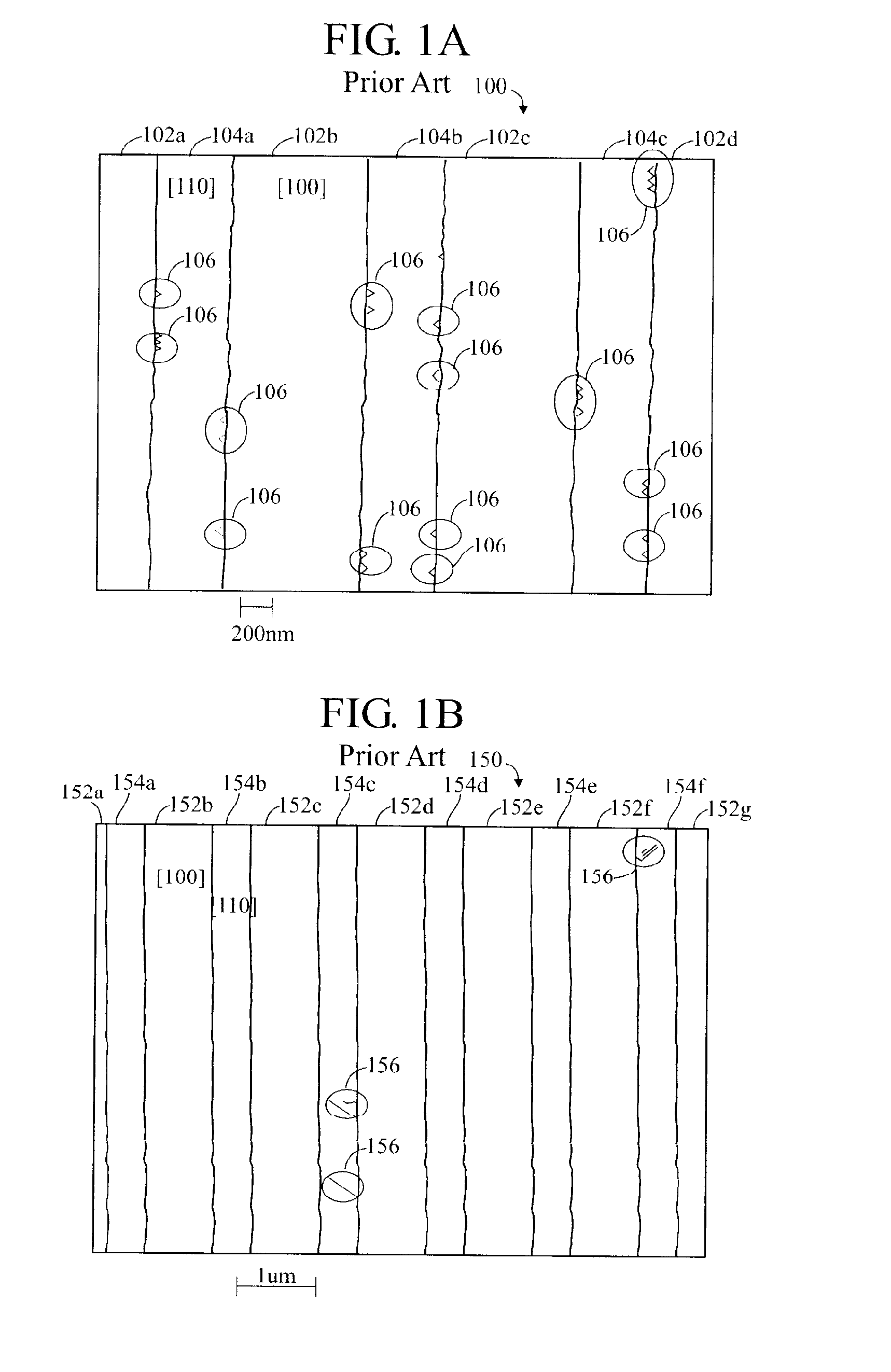
However, data has shown that the re-grown region typically suffers from significantly increased defects.
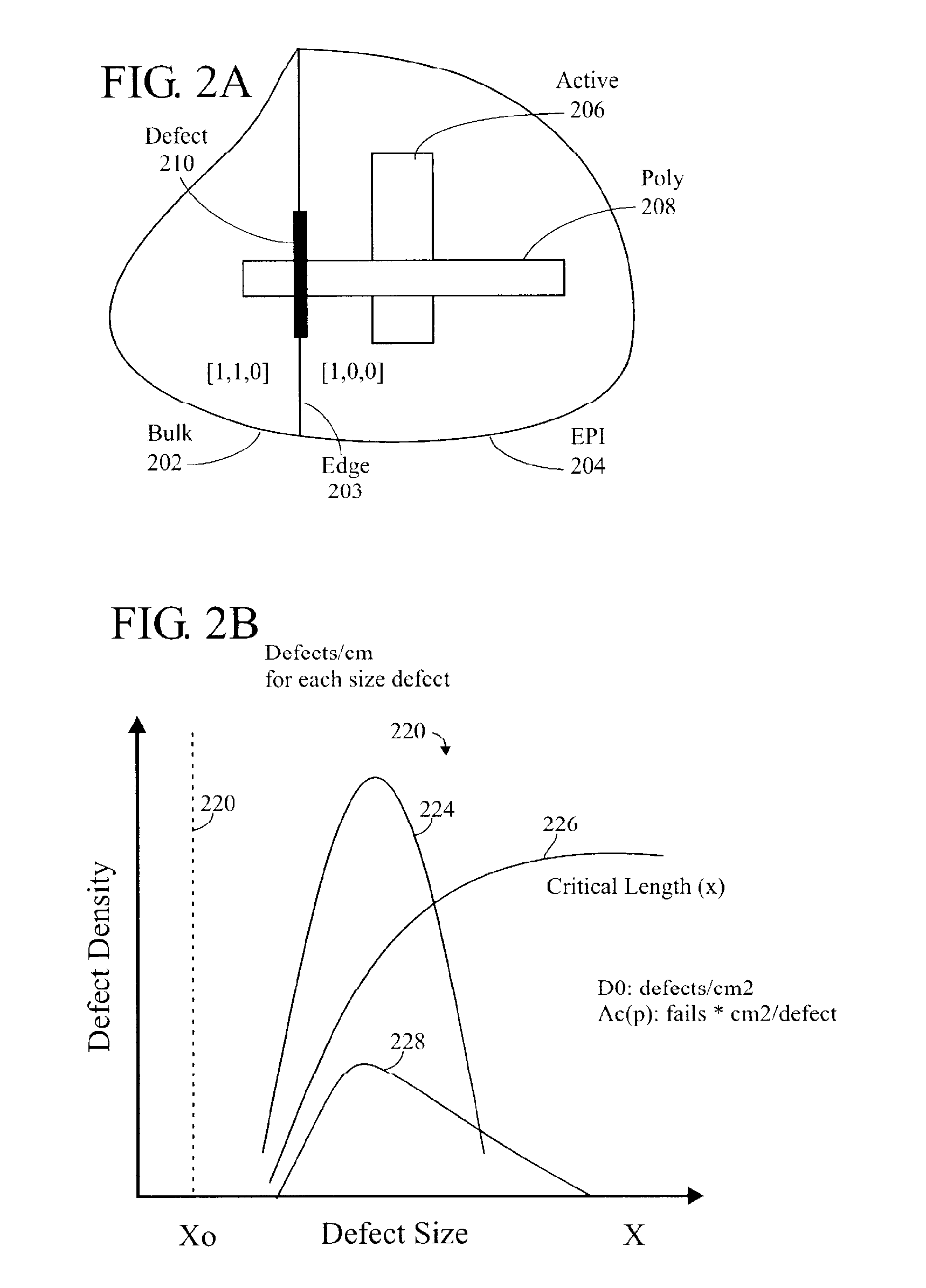
These defects typically extend from the interface between the two differently crystal-oriented substrates into the re-grown region, potentially cause “device leakages” which are harmful to the devices in the re-grown region.
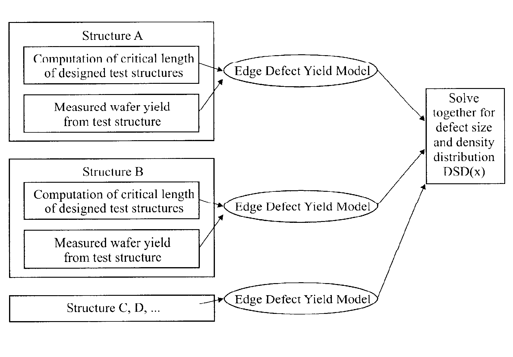
These defects almost always happen at the edge of the EPI (epitaxial, re-grown) region, and they cannot be modeled by the conventional yield model.

Method used


Image

  • Test structures and methodology for detecting hot defects
  • Test structures and methodology for detecting hot defects
  • Test structures and methodology for detecting hot defects

Examples


Embodiment Construction

[0083]Throughout the descriptions set forth herein, lowercase numbers or letters may be used, instead of subscripts. For example Vg could be written Vg. Generally, lowercase is preferred to maintain uniform font size.) Regarding the use of subscripts (in the drawings, as well as throughout the text of this document), sometimes a character (letter or numeral) is written as a subscript—smaller, and lower than the character (typically a letter) preceding it, such as “Vs” (source voltage) or “H2O” (water). For consistency of font size, such acronyms may be written in regular font, without subscripting, using uppercase and lowercase—for example “Vs” and “H20”.

[0084]Although various features of the invention may be described in the context of a single embodiment, the features may also be provided separately or in any suitable combination. Conversely, although the invention may be described herein in the context of separate embodiments for clarity, the invention may also be implemented in ...


PUM


Abstract

Test structures for detecting defects arising from hybrid orientation technology (HOT) through detection of device leakage (gate leakage, junction leakage, and sub-threshold leakage), having at least one active region disposed in a re-grown region of a substrate: a layer of oxide; a layer of poly. Some test structures are dog-bone shaped test structure, tower shaped test structure, and inside-hole shaped. A method for detecting HOT defects involves measuring defect size and location in terms of device leakage, such as gate leakage, junction leakage, and sub-threshold leakage. HOT edge defect density and edge defect size distribution may be calculated, and the resulting defect information may be used to calibrate a defect yield model.

Description

FIELD OF THE INVENTION[0001]The invention generally relates to the manufacture of semiconductor devices using hybrid orientation technology (HOT), and more particularly, to a monitoring system for detecting and characterizing various classes of defects, such as edge defects and corner defects, arising from HOT.BACKGROUND OF THE INVENTION[0002]FETs (field effect transistors) are typically fabricated upon semiconductor wafers, such as Si (silicon) wafers, that have a single crystal orientation. In particular, most of today's semiconductor devices are built upon Si having a [100] crystal orientation. They may also be fabricated on an SOI (silicon on insulator) substrate. Other crystal orientations, such as [110] are also used.[0003]Generally, FETs generally have two different polarities, either N-type or P-type, the resulting nomenclature being “NFET” and “PFET”, or variations thereof, respectively. These two polarity types are considered to be opposite to, or “complementary” of each o...

Claims


Application Information

Patent Timeline
Patent Type & Authority Applications(United States)
IPC IPC(8): H01L21/66H01L23/58
CPCH01L22/12H01L2924/0002H01L2924/00
Inventor HSU, LOUIS LU-CHENKIM, BYEONG YEOLOUYANG, XU
Owner IBM CORP
Why Eureka
Try Eureka