Low-temperature cleaning of native oxide

a technology of native oxide and low temperature, applied in the direction of cleaning using liquids, chemical/physical/physical-chemical processes, energy-based chemical/physical/physical-chemical processes, etc., can solve the problem that the concentration of hydrogen radicals provided by commercially available plasma sources is insufficient to provide acceptable cleaning rates, and achieves reduced device size translation, reduced device components, and reduced vertical dimensions

Inactive Publication Date: 2008-11-27
ASM AMERICA INC
View PDF99 Cites 212 Cited by
  • Summary
  • Abstract
  • Description
  • Claims
  • Application Information

AI Technical Summary

Benefits of technology

[0009]Reduced device sizes translate into decreased vertical dimensions of the device components. Because these smaller devices typically have smaller thermal budgets than their larger predecessors, reducing the temperature at which the oxide is baked-off would be an important process improvement. Lower temperatures are also important in applications that are incompatible with higher temperatures, such as epitaxial silicon / silicon-germanium interfaces, in which defects form at high temperatures. Furthermore, a low-temperature bake would improve reactor throughput because reduced heating and cooling times are needed.

Problems solved by technology

The principal drawback of this method is that the concentration of hydrogen radicals provided by commercially available plasma sources is insufficient to provide acceptable cleaning rates at lower temperatures, in part, because the high silicon-oxygen bond strength limits the efficiency of the reduction reaction.

Method used


Image

  • Low-temperature cleaning of native oxide
  • Low-temperature cleaning of native oxide
  • Low-temperature cleaning of native oxide

Examples


Embodiment Construction

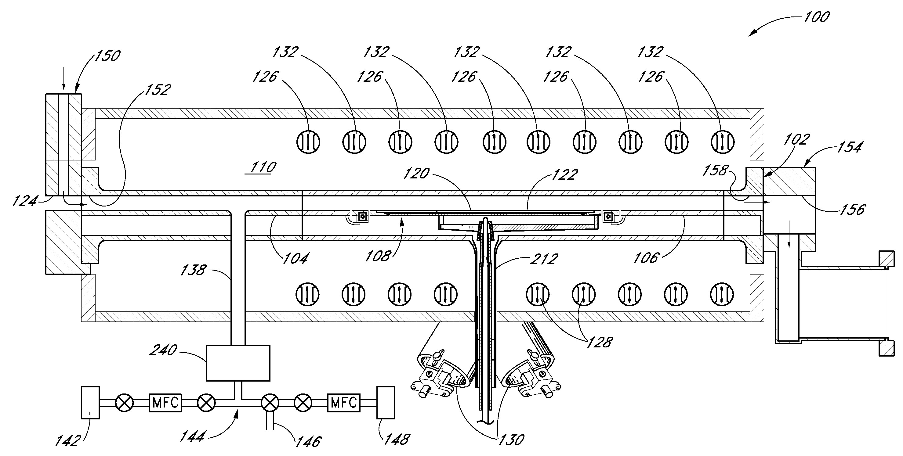
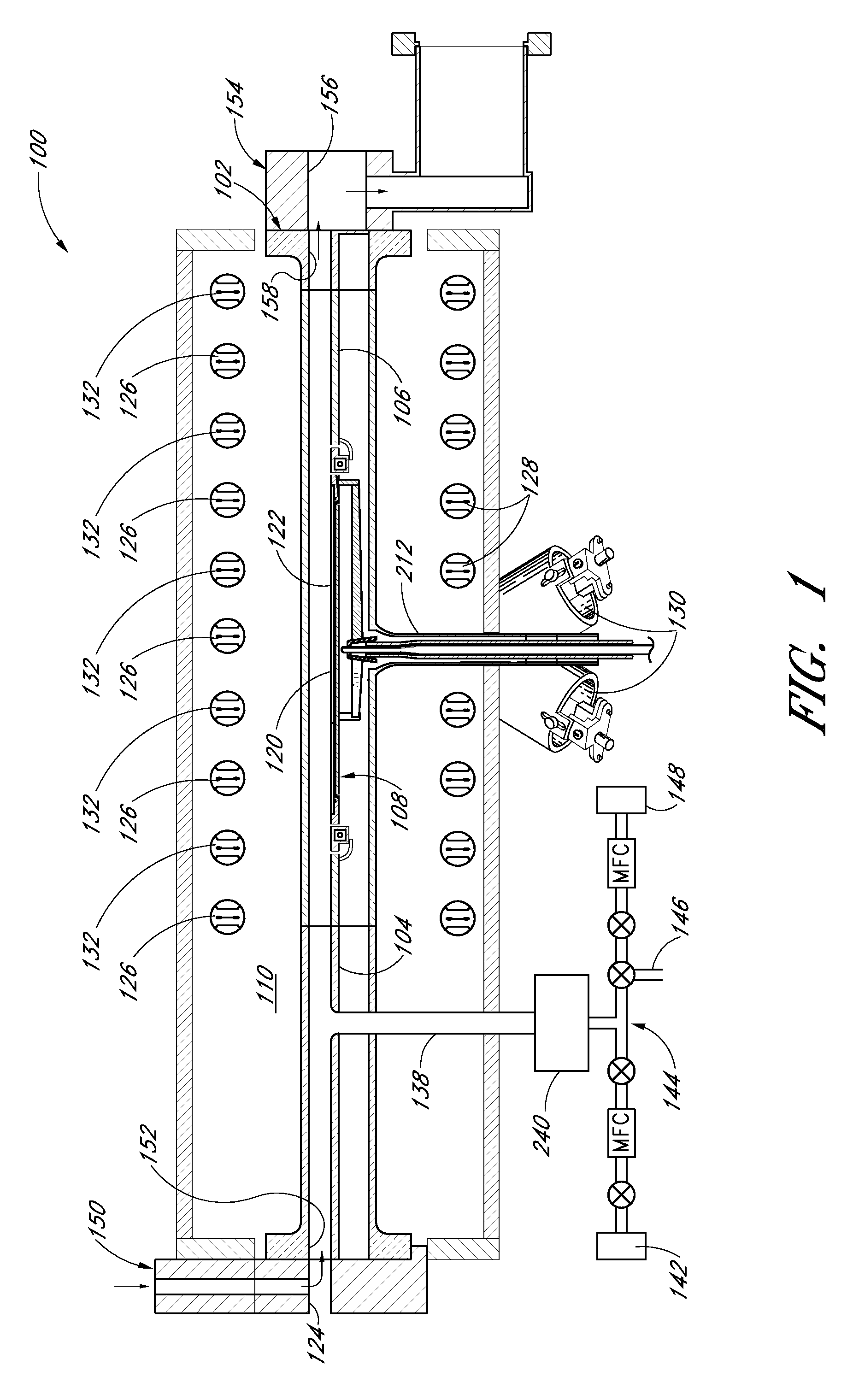
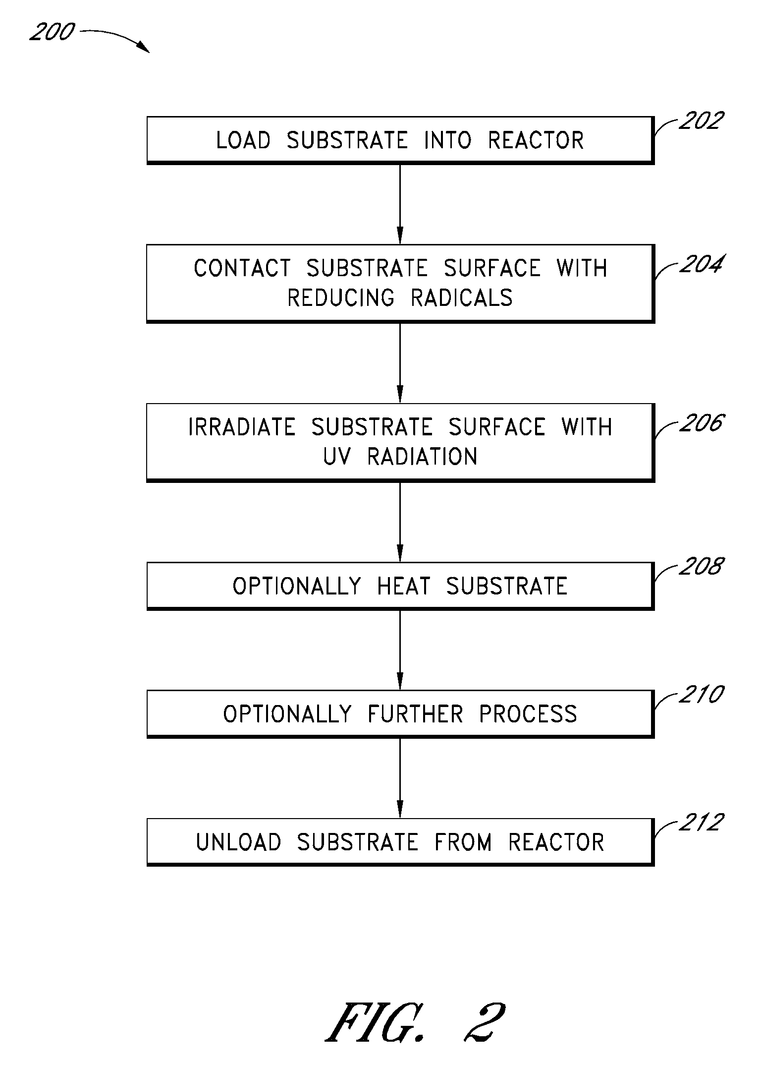
[0029]The disclosed method, apparatus, and systems are useful for cleaning oxide from a surface of a substrate during semiconductor fabrication using radicals, for example, remotely generated, and UV radiation at reduced temperatures. For silicon surfaces, the cleaning provides a silicon surface terminated with hydrogen, a passivated surface stable to about 500-550° C. At higher temperatures, the hydrogen desorbs from the surface. The passivated surface resists oxidation.

[0030]FIG. 1 illustrates a preferred embodiment of a reactor 100 useful for cleaning native oxide. The illustrated reactor 100 is a single-substrate, horizontal flow, cold-wall reactor. Reactors of this type provide improved process control and uniformity compared with batch systems. Such reactors may process only a single, or at most, a handful of substrates at a time, however, reducing throughput. In a batch processing configuration, the substrates are preferably laterally arrayed, facilitating irradiation of the ...


PUM

PropertyMeasurementUnit
temperatureaaaaaaaaaa

Abstract

Disclosed herein is a method of cleaning oxide from a surface in the fabrication of an integrated device using reducing radicals and UV radiation. For silicon surfaces, the cleaning may be performed at a temperature at which a hydrogen-terminated passivated surface is stable, such that the surface remains protected after loading into the chamber until the cleaning is performed. Performing the cleaning at a lower temperature also consumes a reduced portion of the thermal budget of a semiconductor device. Epitaxial deposition can then be performed over the cleaned surface.

Description

BACKGROUND [0001]1. Technical Field[0002]The present disclosure relates to the manufacture of semiconductor devices, and, in particular, to the cleaning of oxide from surfaces during semiconductor fabrication, and for apparatuses therefor.[0003]2. Description of the Related Art[0004]Surfaces of semiconductor substrates on which epitaxial films of silicon or other materials are grown are preferably oxide free. An oxide layer, also referred to as a native oxide layer, typically forms when a clean surface of a semiconductor, and in particular, silicon, is exposed to air. Oxide layers also form on the surfaces of other materials used in integrated device fabrication, for example conductors such as copper. Native oxide on semiconductor surfaces is typically removed prior to deposition using one or more wet cleaning steps. A common method of wet cleaning silicon wafers is performed as follows. An RCA Standard Clean-1 (SC-1) procedure is first performed, which uses a mixture of aqueous amm...

Claims


Application Information

Patent Timeline
Patent Type & Authority Applications(United States)
IPC IPC(8): B08B11/00B01J19/08B08B7/00
CPCB08B7/0057C23C16/0236C23C16/482H01L21/02046H01L21/67115
Inventor ARENA, CHANTAL J.
Owner ASM AMERICA INC
Why Eureka
Try Eureka