Semiconductor device and method for manufacturing the same

a semiconductor and semiconductor technology, applied in the direction of instruments, soldering devices, photomechanical devices, etc., can solve the problems of mounting restrictions, increased size, cost, etc., and achieve the effect of reducing the manufacturing cost of the device, facilitating processing, and ensuring the strength of the second substra

Inactive Publication Date: 2008-11-27
DENSO CORP
View PDF28 Cites 69 Cited by
  • Summary
  • Abstract
  • Description
  • Claims
  • Application Information

AI Technical Summary

Benefits of technology

[0016]The above method provides the semiconductor device, dimensions of which can be minimized, and a manufacturing cost of the device is reduced. Further, strength of the second substrate can be secured. Further, the second substrate can be easily processed by a conventional processing method, so that the manufacturing cost of the device is also reduced.

Problems solved by technology

The chip size accordingly increases to cause a cost problem.
As seen from FIG. 26B, the above-mentioned structure makes face down bonding (ball bonding) difficult, causing mounting restrictions.

Method used


Image

  • Semiconductor device and method for manufacturing the same
  • Semiconductor device and method for manufacturing the same
  • Semiconductor device and method for manufacturing the same

Examples


first embodiment

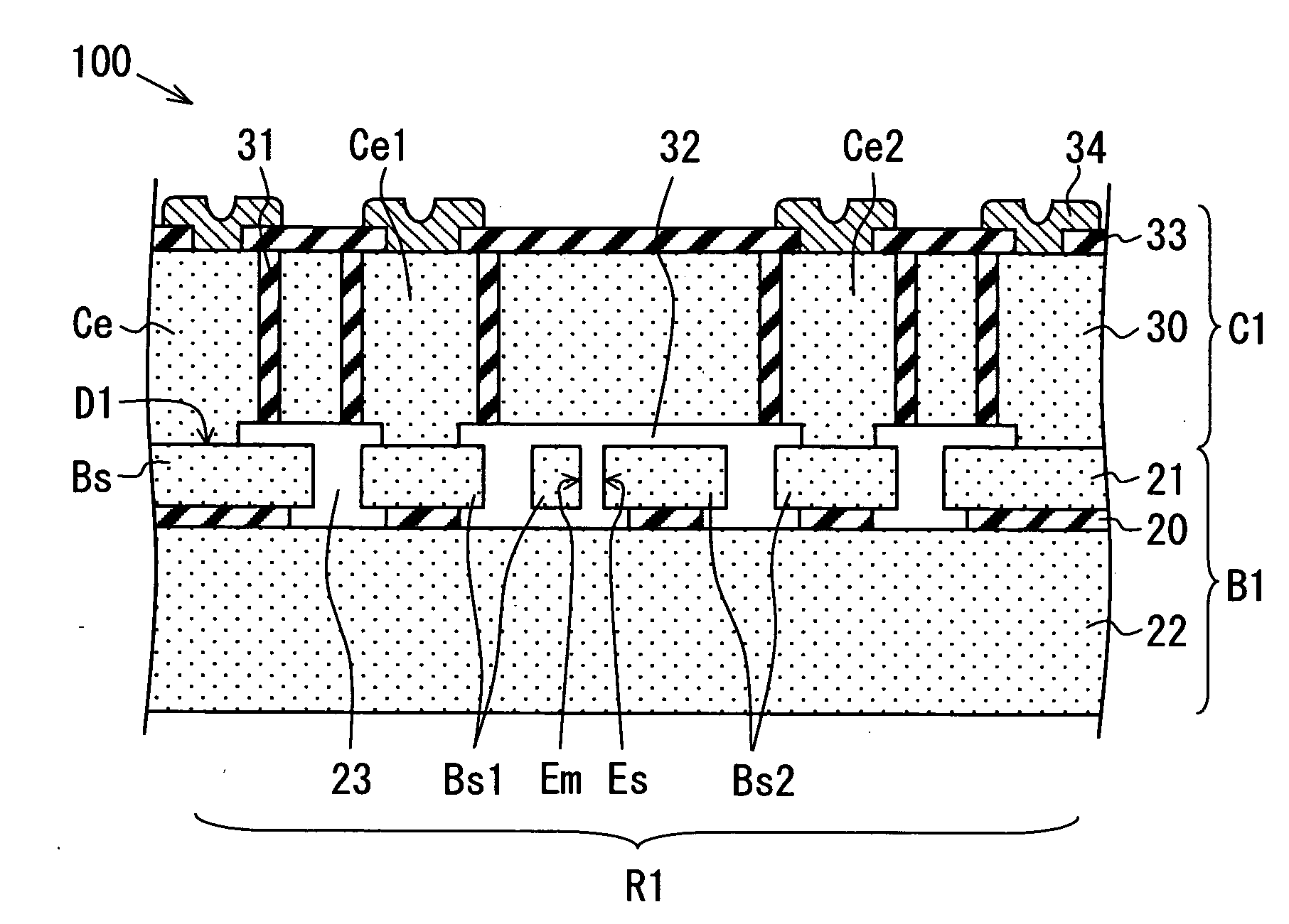
[0044]FIG. 1 is a cross sectional view of a semiconductor device 100 as an example of the semiconductor device according to an embodiment.

[0045]The semiconductor device 100 in FIG. 1 includes a semiconductor base substrate B1 and a conductive cap substrate C1 bonded to the base substrate B1.

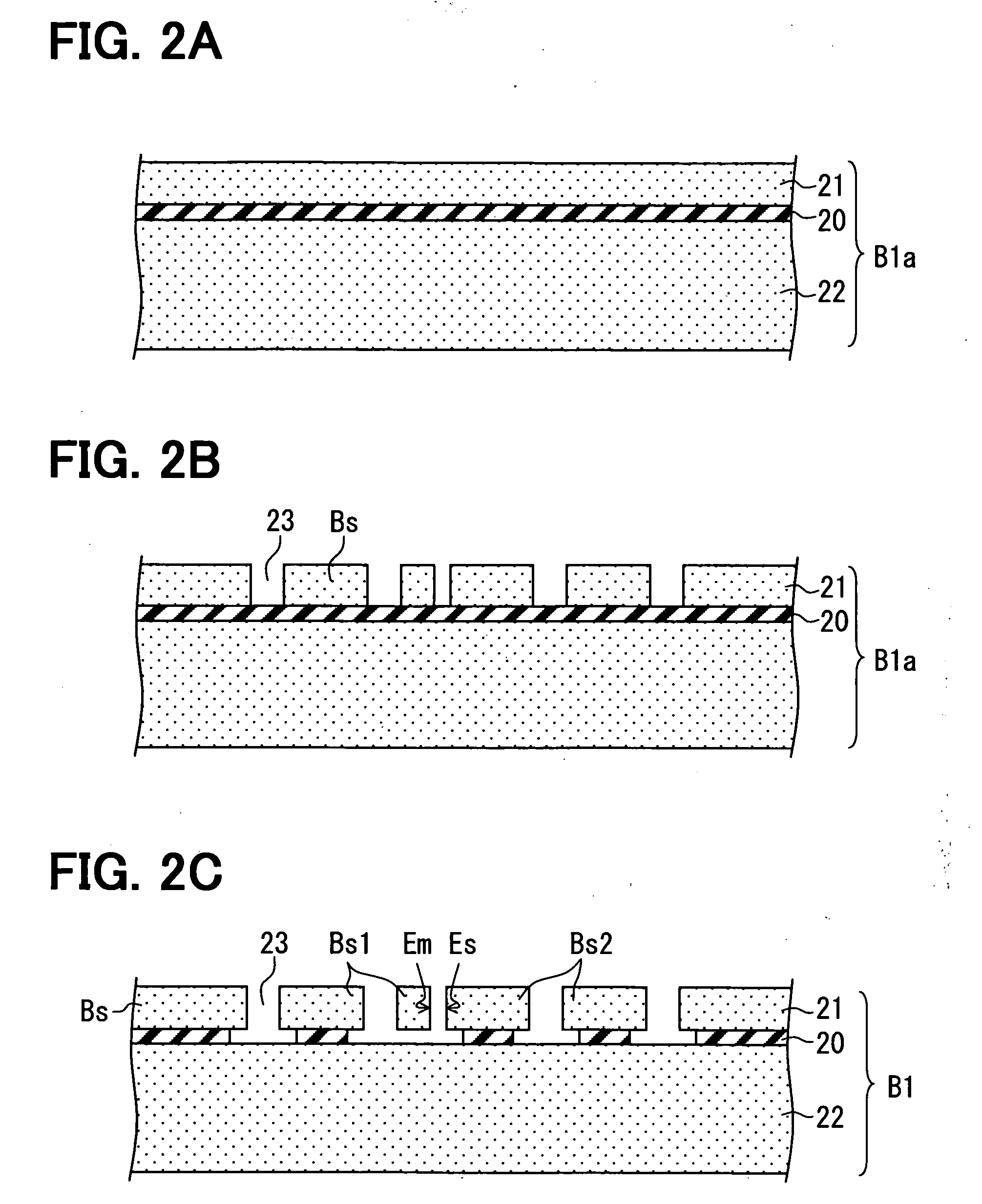
[0046]The base substrate B1 of the semiconductor device 100 in FIG. 1 is an SOI (Silicon On Insulator) substrate including an embedded oxide film 20. The base substrate B1 includes the embedded oxide film 20 sandwiched between an SOI layer 21 and a support substrate 22. Insulated and separated multiple base semiconductor regions Bs are formed on a surface layer of the base substrate B1. The base semiconductor region Bs of the semiconductor device 100 in FIG. 1 belongs to the SOI layer 21 and is insulated and separated from adjacencies by a trench 23 that reaches the embedded oxide film 20.

[0047]The semiconductor device 100 in FIG. 1 is similar to the semiconductor device (inertia force sensor) in...


PUM

PropertyMeasurementUnit
thicknessaaaaaaaaaa
thicknessaaaaaaaaaa
thicknessaaaaaaaaaa

Abstract

A semiconductor device includes: a first substrate made of semiconductor and having first regions, which are insulated from each other and disposed in the first substrate; and a second substrate having electric conductivity and having second regions and insulation trenches. Each insulation trench penetrates the second substrate so that the second regions are insulated from each other. The first substrate provides a base substrate, and the second substrate provides a cap substrate. The second substrate is bonded to the first substrate so that a sealed space is provided between a predetermined surface region of the first substrate and the second substrate. The second regions include an extraction conductive region, which is coupled with a corresponding first region.

Description

CROSS REFERENCE TO RELATED APPLICATIONS[0001]This application is based on Japanese Patent Applications No. 200742619 filed on Feb. 22, 2007, and No. 2007-257840 filed on Oct. 1, 2007, the disclosures of which are incorporated herein by reference.FIELD OF THE INVENTION[0002]The present invention relates to a semiconductor device and a method for manufacturing a semiconductor device.BACKGROUND OF THE INVENTION[0003]For example, JP-2004-333133 A (Patent Document 1) and U.S. Pat. No. 6,936,491 (Patent Document 2) each disclose a semiconductor device and its manufacturing method in which a sealing cap is provided for each of various elements formed on a surface layer of a semiconductor base substrate so as to protect the elements.[0004]FIGS. 26A and 26B show a semiconductor device (inertia force sensor) disclosed in Patent Document 1. FIG. 26A is a top view of the inertia force sensor. FIG. 26B is a cross sectional view taken in the line XXVIB-XXVIB of FIG. 26A. In the following descript...

Claims


Application Information

Patent Timeline
Patent Type & Authority Applications(United States)
IPC IPC(8): H01L21/50H01L23/02B81B3/00B81C3/00H01L21/76H01L27/12H01L29/84
CPCB81B7/007H01L21/76898H01L23/481H01L2924/0002H01L2924/00012H01L2924/00
Inventor FUJII, TETSUOSUGIURA, KAZUHIKO
Owner DENSO CORP
Why Eureka
Try Eureka