Electron device using oxide semiconductor and method of manufacturing the same

a technology of oxide semiconductor and electron, applied in the field of electron devices, can solve the problems of deterioration of accuracy, increase of manufacturing cost, and decrease of throughput, and achieve the effects of stable electron, low cost, and simplified manufacturing process

Inactive Publication Date: 2008-11-27
CANON KK
View PDF3 Cites 244 Cited by
  • Summary
  • Abstract
  • Description
  • Claims
  • Application Information

AI Technical Summary

Benefits of technology

[0010]Consequently, the present invention aims to enable simplification of manufacturing processes in plural thin film transistors each using a metal oxide semiconductor, to provide a stable electron device at low cost, and to provide a manufacturing method of the electron device.

Problems solved by technology

Since the dry etching is generally performed by using an expensive vacuum system, it increases manufacturing cost.
However, in the wet etching, there is a case where throughput decreases due to deterioration of accuracy in the micro fabrication process, limitation of device size by absorbed moisture to the channel region by a wet process, addition of a dry process, and the like.

Method used


Image

  • Electron device using oxide semiconductor and method of manufacturing the same
  • Electron device using oxide semiconductor and method of manufacturing the same
  • Electron device using oxide semiconductor and method of manufacturing the same

Examples


first embodiment

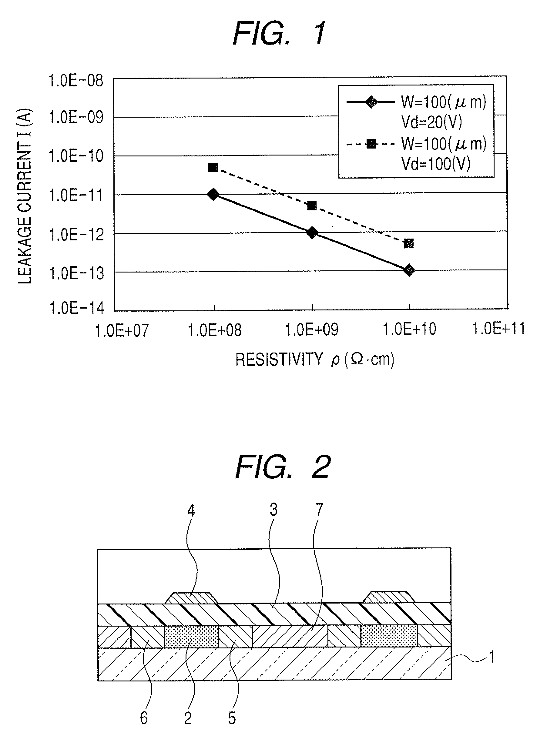
[0032]FIG. 2 is a schematic cross-sectional view indicating the structure of a top gate (coplanar) TFT as an example of a thin film transistor according to the present embodiment.

[0033]A metal oxide layer 7 (high-resistance metal oxide layer) exhibiting the high resistivity equal to or larger than 1010 Ω·cm is provided on a substrate 1. A semiconductor region 2 is provided by decreasing the resistance of a part of the metal oxide layer 7, and a device separation region and a channel region are formed. Furthermore, a source region 6 and a drain region 5 are provided by decreasing the resistance more than that in the semiconductor region. In this case, it is desirable to fix a resistance value within a range from a vale equal to or larger than 103 Ω·cm to a value equal to or less than 107 Ω·cm. By adopting this resistance value, the field effect mobility equal to or larger than 1 cm2 / Vs can be obtained. In addition, it is desirable that the resistance values of the source region and t...

second embodiment

TFT

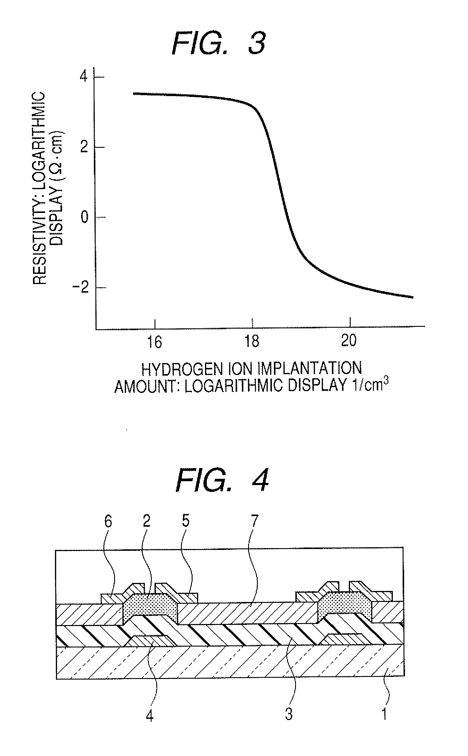
[0037]FIG. 4 is a schematic cross-sectional view indicating the structure of a bottom gate (inverse staggered) TFT as an example of a TFT according to the present embodiment.

[0038]The gate electrode 4 is provided on the substrate 1, the gate insulation film 3 is provided on the gate electrode 4 and the metal oxide layer 7 (high-resistance metal oxide layer) exhibiting the high resistivity equal to or larger than 1010 Ω·cm is further provided on the gate insulation film 3. The semiconductor region 2 is provided by decreasing the resistance of a part of the metal oxide layer 7, and a device separation region and a channel region are formed. An inverse staggered TFT is constituted by providing the source electrode 6 and the drain electrode 5 on this processed layer. In this case, similar to the first embodiment, it is desirable to fix a resistance value within a range from a value equal to or larger than 103 Ω·cm to a value equal to or less than 107 Ω·cm. By adopting this resistance...

third embodiment

s

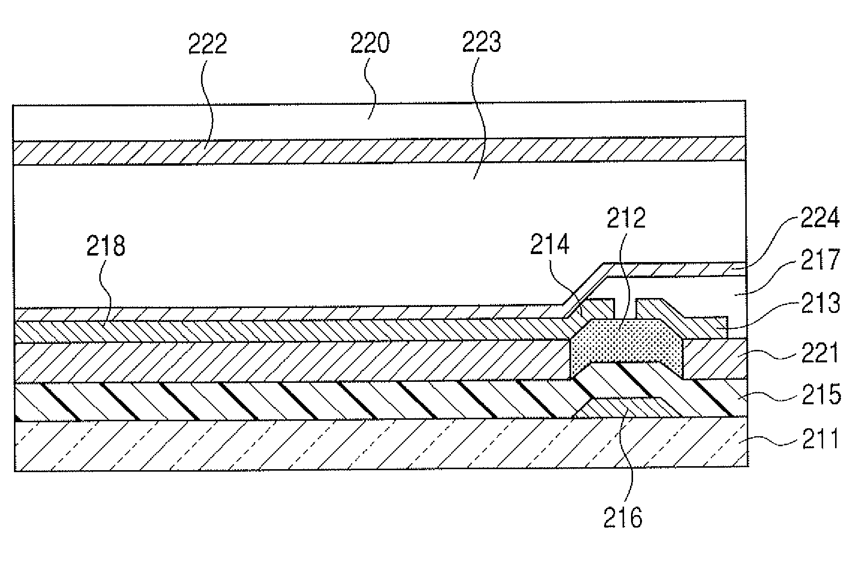
[0041]A display apparatus can be constituted by connecting the drain electrodes serving as output terminals of the thin film transistors of the above-mentioned second embodiment with electrodes of display devices such as liquid crystal devices, organic or inorganic EL devices. Hereinafter, an example of specific display apparatus structure will be described by using a cross-sectional view of the display apparatus.

[0042]FIG. 5 is a cross-sectional view indicating an example of the display apparatus.

[0043]After forming a gate electrode 116 and a gate insulation film 115 on a base 111, a metal oxide layer 121 (high resistance metal oxide layer) of the present invention exhibiting the high resistivity is formed. In addition, after forming a source electrode 113 and a drain electrode 114, a channel region 112 is formed by decreasing the resistance of a part of the metal oxide layer by performing an annealing process in the inert gas, thereby forming a TFT. An electrode 118 is connected ...


PUM


Abstract

In an electron device in which plural thin film transistors each having at least a source electrode, a drain electrode, a semiconductor region including a channel, a gate insulation film and a gate electrode are provided on a substrate, a device separation region provided between the plural thin film transistors and the semiconductor region are constituted by a same metal oxide layer, and resistance of the semiconductor region is formed to be lower than resistance of the device separation region.

Description

BACKGROUND OF THE INVENTION[0001]1. Field of the Invention[0002]The present invention relates to an electron device in which plural thin film transistors each using an oxide semiconductor (particularly, a metal oxide semiconductor) are provided, and a method of manufacturing the relevant electron device. The electron device like this is generally used for a display device such as an electroluminescent (EL) device or a liquid crystal cell.[0003]2. Description of the Related Art[0004]In recent years, as described in Japanese Patent Application Laid-Open No. 2002-076356, a thin film transistor (TFT) in which a transparent conductive metal oxide polycrystalline thin film using ZnO as its main component is used as the channel layer has been actively developed.[0005]Since the transparent conductive metal oxide polycrystalline thin film can be deposited at low temperature and is transparent in relation to visible light, it is possible by using the relevant film to form a flexible transpare...

Claims


Application Information

Patent Timeline
Patent Type & Authority Applications(United States)
IPC IPC(8): H01L21/00
CPCH01L27/1225H01L29/7869
Inventor HAYASHI, RYOSANO, MASAFUMI
Owner CANON KK
Why Eureka
Try Eureka