Shallow junction formation and high dopant activation rate of MOS devices

a technology of mos devices and dopants, which is applied in the direction of mos devices, transistors, electrical equipment, etc., can solve the problems of reducing the junction depth of mos devices accordingly, affecting the effect of implantation dosage, and affecting the formation process, so as to achieve the effect of reducing the junction depth and improving the short channel characteristics

Inactive Publication Date: 2008-11-27
TAIWAN SEMICON MFG CO LTD
View PDF5 Cites 17 Cited by
  • Summary
  • Abstract
  • Description
  • Claims
  • Application Information

AI Technical Summary

Benefits of technology

[0007]The advantageous features of the present invention include reduced junction depth

Problems solved by technology

The junction depths of the MOS devices are also reduced accordingly, which causes technical difficulties for the formation processes.
However, it is difficult to increase implantation dosages without causing the adverse increase in junction depth.
However, arsenic has a low activation rate.
Therefore, designers have to compromise between

Method used


Image

  • Shallow junction formation and high dopant activation rate of MOS devices
  • Shallow junction formation and high dopant activation rate of MOS devices
  • Shallow junction formation and high dopant activation rate of MOS devices

Examples


Embodiment Construction

[0010]The making and using of the presently preferred embodiments are discussed in detail below. It should be appreciated, however, that the present invention provides many applicable inventive concepts that can be embodied in a wide variety of specific contexts. The specific embodiments discussed are merely illustrative of specific ways to make and use the invention, and do not limit the scope of the invention.

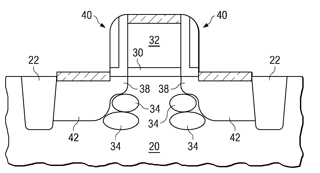
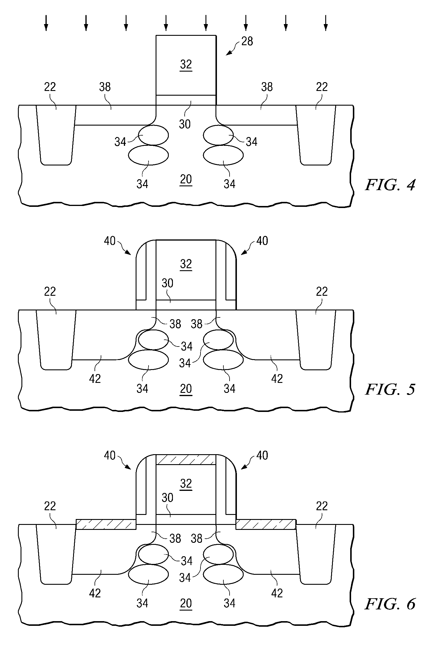
[0011]A method for forming an n-type metal-oxide-semiconductor (MOS) device is provided. The intermediate stages of manufacturing embodiments of the present invention are illustrated. Throughout various views and illustrative embodiments of the present invention, like reference numbers are used to designate like elements.

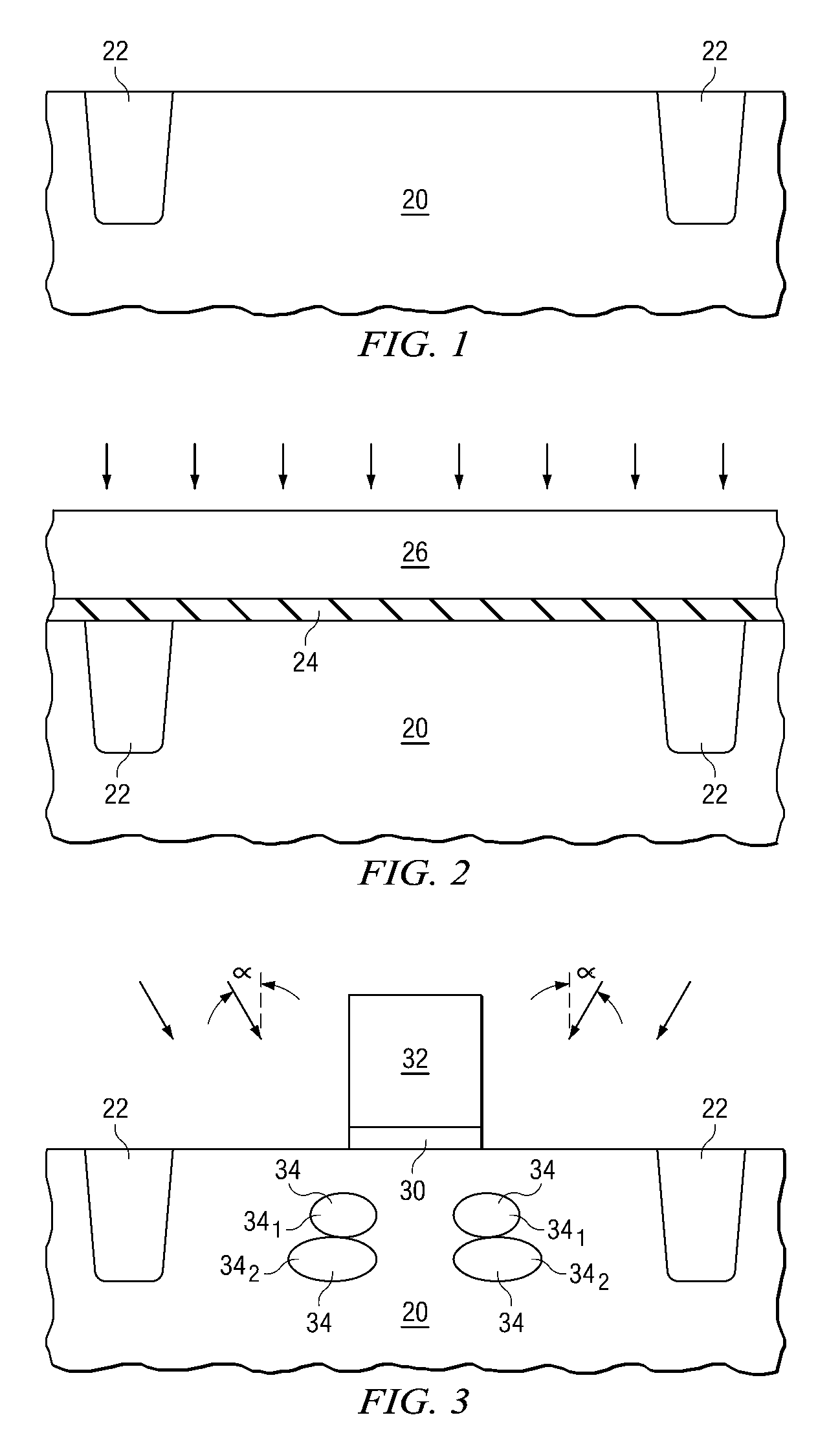
[0012]Referring to FIG. 1, substrate 20 is provided. Substrate 20 preferably includes bulk silicon, although other commonly used structures and semiconductor materials such as silicon-on-insulator (SOI) and silicon alloys can be used. Preferably, substrate 20...


PUM


Abstract

A method for forming a semiconductor structure includes providing a semiconductor substrate; forming a gate stack over the semiconductor substrate; implanting carbon into the semiconductor substrate; and implanting an n-type impurity into the semiconductor substrate to form a lightly doped source/drain (LDD) region, wherein the n-type impurity comprises more than one phosphorous atom. The n-type impurity may include phosphorous dimer or phosphorous tetramer.

Description

TECHNICAL FIELD[0001]This invention relates generally to semiconductor devices, and more particularly to the structure and fabrication methods of metal-oxide-semiconductor devices.BACKGROUND[0002]With the scaling down of integrated circuits, metal-oxide-semiconductor (MOS) devices are becoming increasingly smaller. The junction depths of the MOS devices are also reduced accordingly, which causes technical difficulties for the formation processes. For example, small MOS devices demand high impurity concentrations in source / drain regions and lightly doped source and drain (LDD) regions in order to reduce sheet resistances. However, it is difficult to increase implantation dosages without causing the adverse increase in junction depth.[0003]Conventionally, arsenic is implanted in the formation of LDD regions. Arsenic has a relatively low diffusion length, and thus can be implanted to a high concentration without significantly affecting short channel characteristics and junction abruptn...

Claims


Application Information

Patent Timeline
IPC IPC(8): H01L21/336
CPCH01L21/26506H01L21/26586H01L29/1083H01L29/66492H01L29/665H01L29/6659H01L29/7833H01L21/2658H01L21/26513
Inventor NIEH, CHUN-FENGKU, KEH-CHIANGCHENG, NAI-HANCHEN, CHI-CHUNLIN, LI-TE S.
Owner TAIWAN SEMICON MFG CO LTD
Why Eureka
Try Eureka