Etching solution, method of surface modification of semiconductor substrate and method of forming shallow trench isolation

Active Publication Date: 2008-12-04
MACRONIX INT CO LTD
View PDF7 Cites 0 Cited by
  • Summary
  • Abstract
  • Description
  • Claims
  • Application Information

AI Technical Summary

Benefits of technology

[0008]The invention is directed to an etching solution, a method of surface modification of a semiconductor substrate and a method of forming shallow trench isolation. The etching solution includes an oxidant and an oxide remover. The surface of the semiconductor subst

Problems solved by technology

As a result, the following manufacturing processes of the semiconductor device are affected seriously.
However, when the mask layer is removed by wet etching, the etchant erodes the silicon or polysilicon of the silicon chip and damages the surface of the silicon chip.
Additionally, after the mask layer is removed, n

Method used


Image

  • Etching solution, method of surface modification of semiconductor substrate and method of forming shallow trench isolation
  • Etching solution, method of surface modification of semiconductor substrate and method of forming shallow trench isolation
  • Etching solution, method of surface modification of semiconductor substrate and method of forming shallow trench isolation

Examples


Example

[0023]A preferred embodiment is provided as follow to illustrate the present invention. However, the present invention is not limited thereto. Furthermore, unnecessary components are not shown in the drawings of the embodiment for clarity.

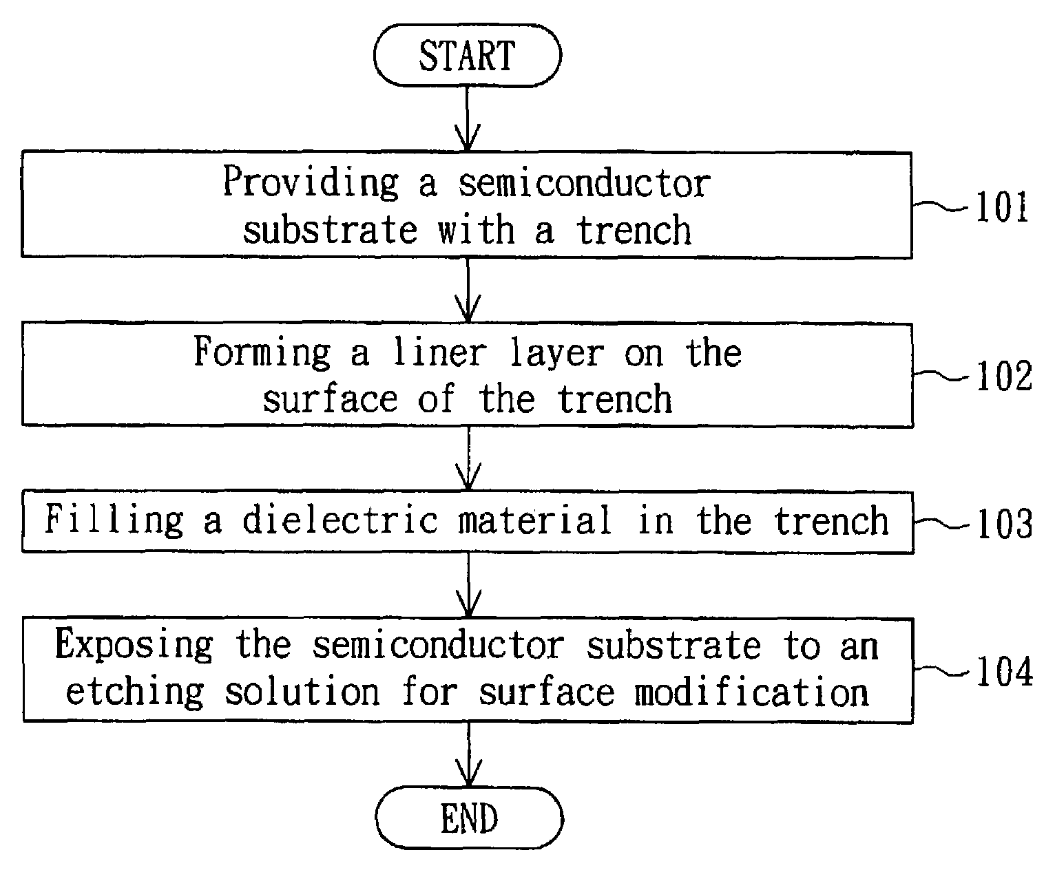
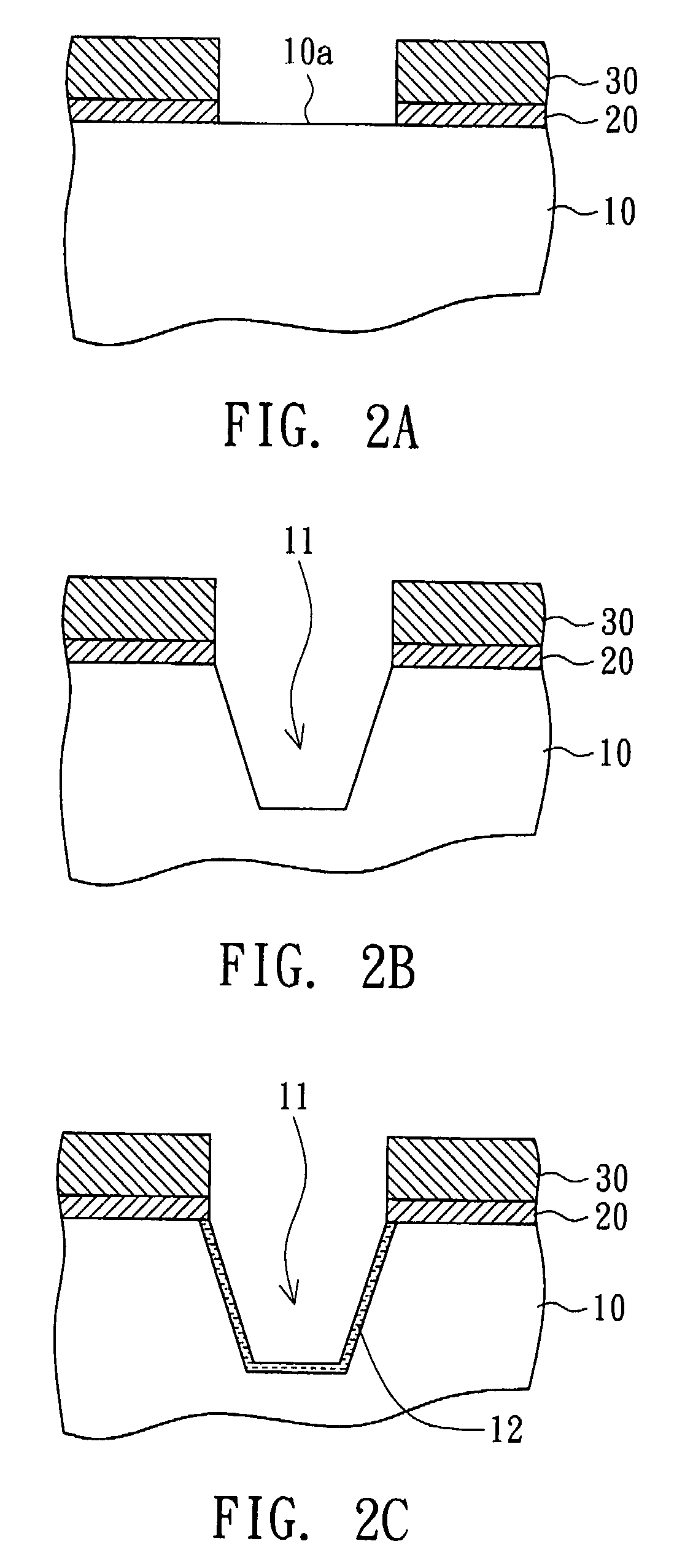
[0024]Please refer to FIG. 1. FIG. 1 is a flow chart of a method of forming shallow trench isolation according to a preferred embodiment of the present invention. The method mainly includes the following steps. First, a semiconductor with a trench is provided. Next, a liner layer is formed on the surface of the trench. Then, a dielectric material is filled in the trench. Afterwards, the semiconductor substrate is exposed to an etching solution for surface modification to improve the surface quality of the semiconductor substrate, and to avoid kooi effect.

[0025]The method is further exemplified by forming shallow trench isolation at a silicon substrate in the following description. However, any one who is skilled in the technology of the invention w...


PUM


Abstract

An etching solution, a method of surface modification of a semiconductor substrate and a method of forming shallow trench isolation are provided. The etching solution is used for surface modifying the semiconductor substrate. The etching solution includes an oxidant and an oxide remover. The semiconductor substrate is oxidized to a semiconductor oxide by the oxidant, and the oxide remover subtracts the semiconductor oxide.

Description

BACKGROUND OF THE INVENTION[0001]1. Field of the Invention[0002]The invention relates in general to an etching solution, a method of surface modification of a semiconductor substrate and a method of forming shallow trench isolation, and more particularly to an etching solution, a method of surface modification of a semiconductor substrate and a method of forming shallow trench isolation applied to a silicon substrate.[0003]2. Description of the Related Art[0004]As the scale of integrated circuits decreases, the isolation process between the semiconductor devices to avoid current leakage or short circuit becomes more and more important. Conventionally, a local oxidation of silicon (LOCOS) isolation method is introduced to isolate semiconductor devices. The LOCOS isolation method mainly includes following steps. First, a pad oxide layer and a pad nitride layer are formed on a silicon chip. Next, the pad oxide layer and the pad nitride layer are etched to expose a part of the silicon c...

Claims


Application Information

Patent Timeline
IPC IPC(8): H01L21/762C09K13/08H01L21/31
CPCC09K13/08H01L21/30604H01L21/30608H01L21/76232
Inventor WU, CHIA-WEISHIEH, JUNG-YUYANG, LING-WU
Owner MACRONIX INT CO LTD
Why Eureka
Try Eureka