
Field-effect semiconductor device and method of fabrication

a field-effect semiconductor and semiconductor technology, applied in the field of field-effect semiconductor devices, can solve the problems of reducing the electron concentration in the two-dimensional electron gas layer, reducing the efficiency of the associated electric circuit, and reducing the use of the conventional normally-on hemt, so as to reduce the gate leak current, reduce the resistance, and eliminate the effect of fluctuations from one device to another

Inactive Publication Date: 2008-12-11
SANKEN ELECTRIC CO LTD
View PDF20 Cites 33 Cited by
  • Summary
  • Abstract
  • Description
  • Claims
  • Application Information

AI Technical Summary

Benefits of technology

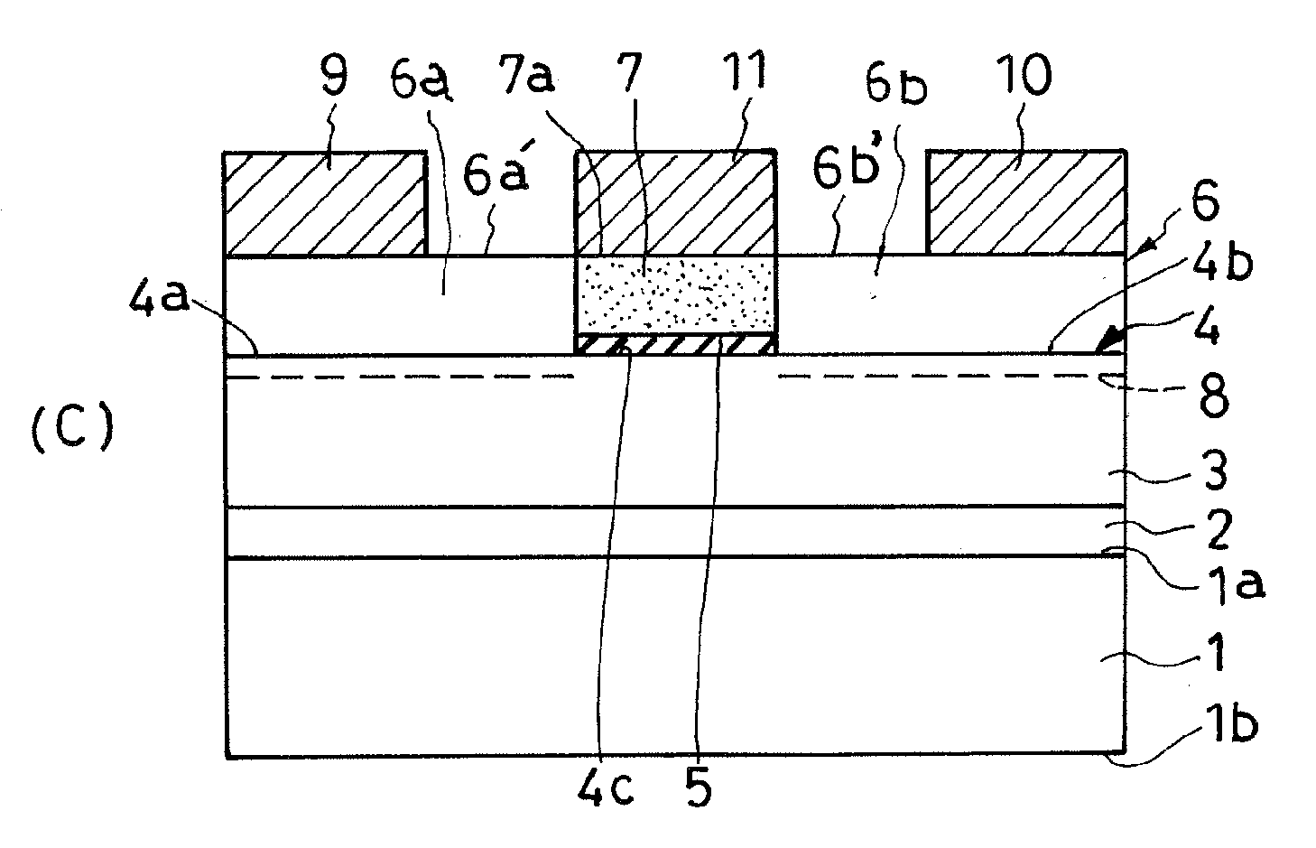
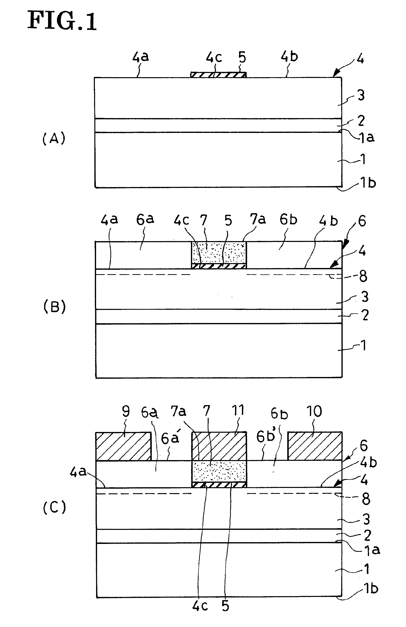
The present invention is about making field-effect semiconductor devices that can normally-off operate. The invention aims to reduce the performance characteristics of such devices to an absolute minimum. The invention also includes a method of fabricating the normally-off field-effect semiconductor device, which involves the deposition of a second semiconductor material on the major surface of a first semiconductor layer, creating a two-dimensional carrier gas layer in the first semiconductor layer. The invention provides a simple and easy-to-fabricate solution for creating normally-off field-effect semiconductor devices.

Problems solved by technology

Use of such a negative power supply made the associated electric circuitry unnecessary complex and expensive.
The conventional normally-on HEMT was therefore rather inconvenient of use.
A thinner electron supply layer weakens the field of the electron supply layer due to piezoelectric and spontaneous depolarizations, resulting in the diminution of electron concentration in the two-dimensional electron gas layer.
However, the normally-off HEMT based upon this conventional scheme proved to possess the drawback that, by reason of the thin electron supply layer itself, the two-dimensional electron supply layer suffers an unnecessary drop in electron concentration at other than right below the gate as well.
The result was an inconveniently high source-drain turn-on resistance.
This solution proved unsatisfactory in that the creation of the recess by selective etching of the electron supply layer might lead to the impairment of the crystalline structure of the electron supply layer, as well as that of the electron transit layer, and hence to the deterioration of the electrical characteristics of the HEMT.
This prior art device is also objectionable by reason of difficulties in invariably creating the high resistance part of the electron supply layer under the gate electrode.

Method used


Image

  • Field-effect semiconductor device and method of fabrication
  • Field-effect semiconductor device and method of fabrication
  • Field-effect semiconductor device and method of fabrication

Examples


embodiment

of FIG. 2

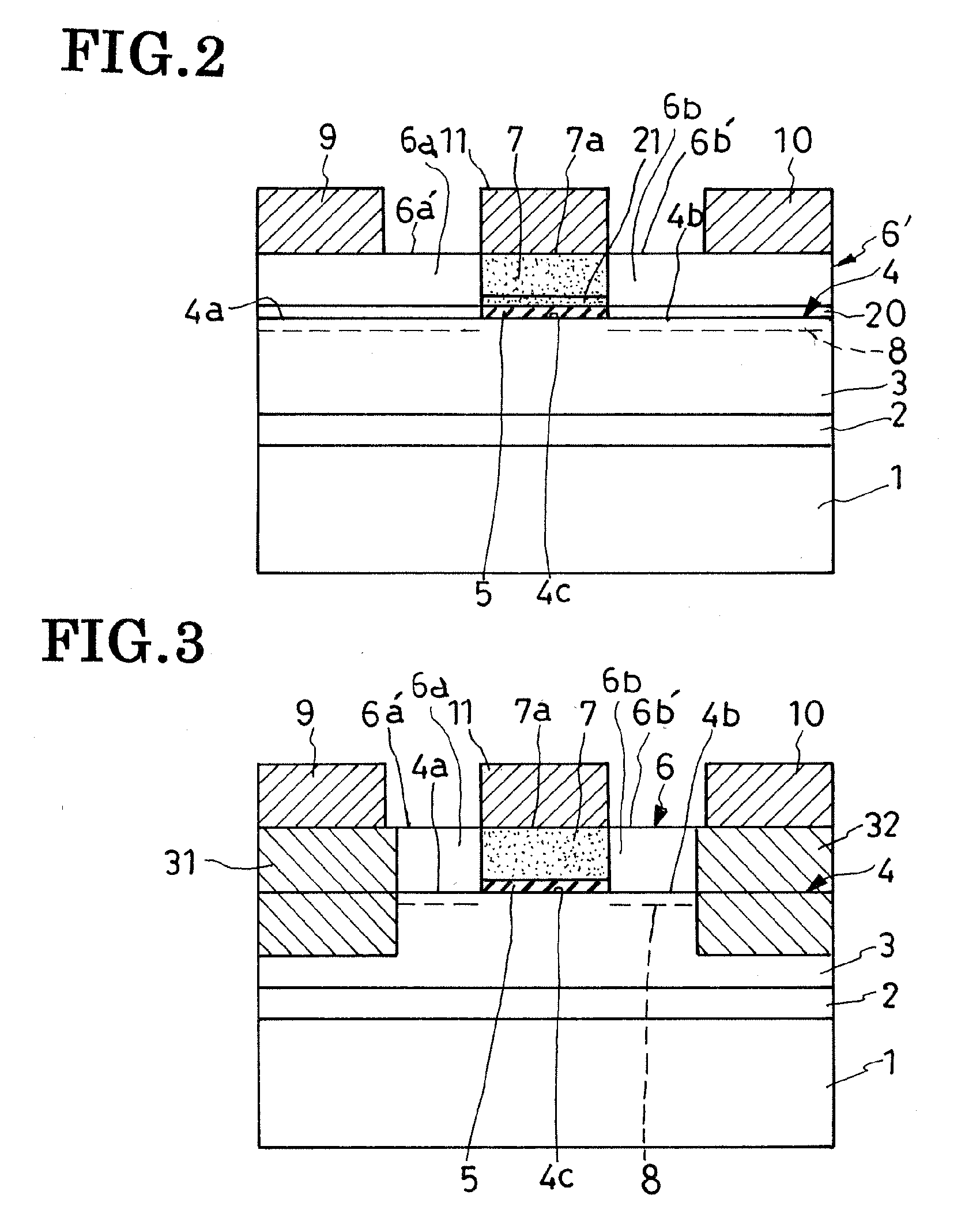
[0047]The second preferred form of HEMT-like field-effect semiconductor device features a modified two-part electron supply layer 6′ and a spacer 20 between the electron transit layer 3 and the modified electron supply layer 6′. All the other details of construction are substantially as set forth above with reference to FIG. 1.

[0048]The modified two-part electron supply layer 6′ together with the discontinuous growth layer 7 is made from any of the n-doped semiconducting nitrides that are generally defined by the formula:

AlaGa1-aN

where the subscript a is a numeral that is greater than zero and less than one, greater than a in the formula above defining the materials for the electron transit layer 3, preferably in the range of 0.2 through 0.4, and most desirably 0.3; or by the formula:

AlaInbGa1-a-bN

where the subscript a is a numeral that is greater than zero and less than one, and greater than a in the formula above defining the materials for the electron transit layer 3; th...


PUM


Abstract

After creating an electron transit layer on a substrate, a baffle is formed on midpart of the surface of the electron transit layer, the surface having a pair of spaced-apart parts left on both sides of the baffle. A semiconducting material different from that of the electron transit layer is deposited on its surface thereby conjointly fabricating an electron supply layer grown continuously on the pair of spaced-apart parts of the electron transit layer surface, and a discontinuous growth layer on the baffle in the midpart of the electron transit layer surface. When no voltage is being impressed to the gate electrode on the discontinuous growth layer, this layer creates a hiatus in the two-dimensional electron gas layer generated along the heterojunction between the electron supply layer and electron transit layer. The hiatus is closed upon voltage application to the gate electrode.

Description

CROSS REFERENCE TO RELATED APPLICATIONS[0001]This application claims priority to Japanese Patent Application No. 2007-154156, filed Jun. 11, 2007.BACKGROUND OF THE INVENTION[0002]This invention relates generally to semiconductor devices, particularly to field-effect semiconductor devices as typified by high electron mobility transistors (HEMTs), and more particularly to such devices that are normally off. The invention also pertains to a method of making such normally-off field-effect semiconductor devices.[0003]The HEMT of typical prior art design comprises an electron transit layer of undoped gallium nitride (GaN) grown on a substrate of silicon, sapphire or the like via a buffer, an electron supply, or barrier, layer of n-doped or undoped aluminum gallium nitride (AlGaN) on the electron transit layer, and a source, drain, and gate (Schottkey) electrode on the electron supply layer. The AlGaN electron supply layer has a greater bandgap and less lattice constant than does the GaN e...

Claims


Application Information

Patent Timeline
Patent Type & Authority Applications(United States)
IPC IPC(8): H01L29/778H01L21/338H01L29/812
CPCH01L29/1029H01L29/2003H01L29/66462H01L29/7787H01L29/78
Inventor SATO, KEN
Owner SANKEN ELECTRIC CO LTD
Learn More