Imaging device, method of driving imaging device, and method of manufacturing imaging device

a technology of imaging device and manufacturing method, which is applied in the direction of radioation control device, television system scanning details, television system, etc., can solve the problems of difficult to form stacked layer uniformity, difficult to secure reliability, and difficult to ensure reliability. the effect of high reliability

Inactive Publication Date: 2008-12-11
FUJIFILM CORP
View PDF5 Cites 14 Cited by
  • Summary
  • Abstract
  • Description
  • Claims
  • Application Information

AI Technical Summary

Benefits of technology

[0010]An object of an illustrative, non-limiting embodiment of the invention is to provide an imaging device that can be applied to an imaging apparatus for consumer use and is highly reliable, a method of driving an imaging device, and a method of manufacturing an imaging device.

Problems solved by technology

As a result, it becomes difficult to secure the reliability, and deviation in a multiplication factor for every pixel occurs and a signal amplified due to machining deviation of the read gate is generated.
Furthermore, in order to realize a high multiplication factor in multiplication in a transfer path, it is necessary to apply a high voltage difference between adjacent electrodes, which causes a problem in the reliability.
Accordingly, it is very difficult to form the stacked layer uniform and it is not put to practical use.
In particular, it was difficult to provide the structure in imaging apparatuses for consumer use, such as a digital camera and a video camera.

Method used


Image

  • Imaging device, method of driving imaging device, and method of manufacturing imaging device
  • Imaging device, method of driving imaging device, and method of manufacturing imaging device
  • Imaging device, method of driving imaging device, and method of manufacturing imaging device

Examples


Embodiment Construction

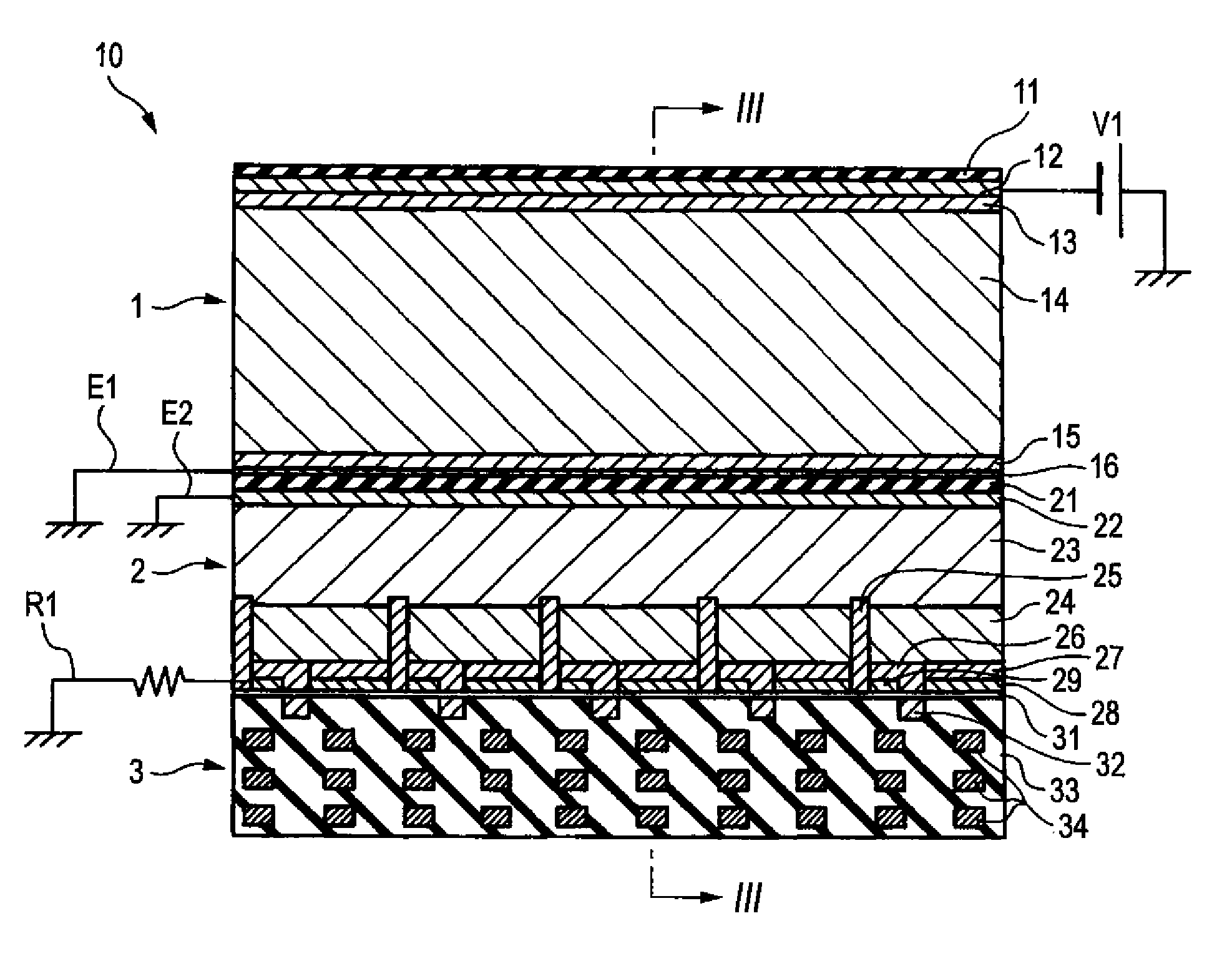
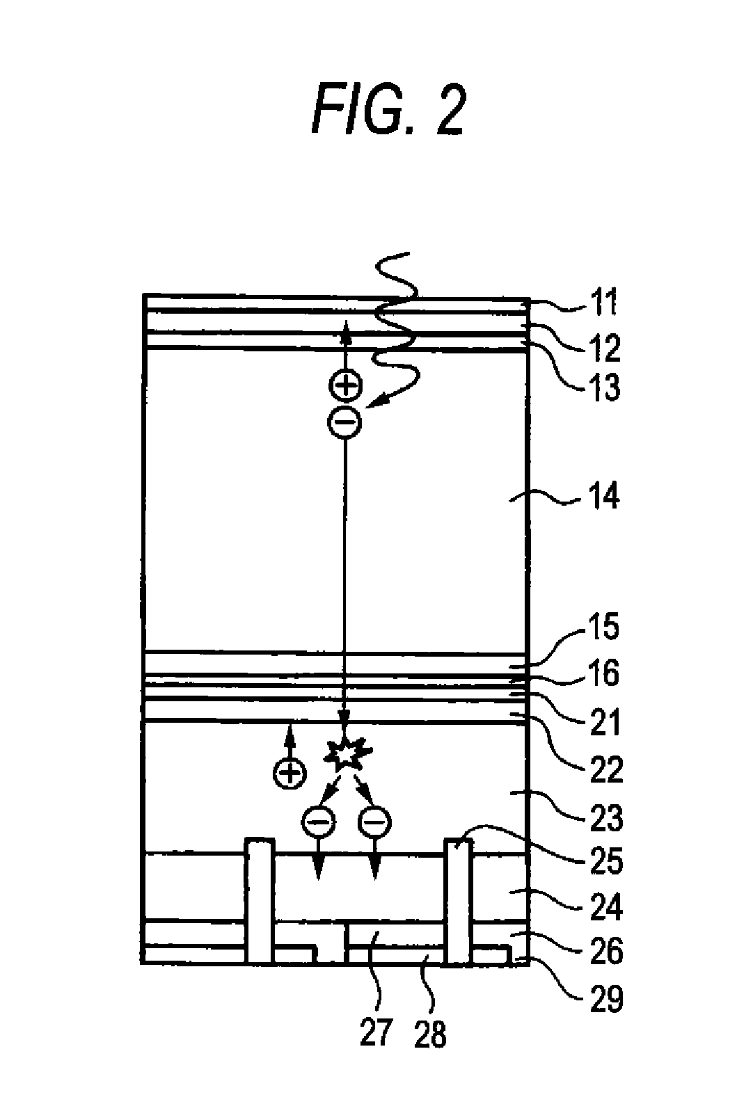
[0044]An imaging device according to an exemplary embodiment of the invention is configured such that an electric field is generated in the electron acceleration layer by applying a voltage to the high-concentration impurity layer formed in the photoelectric conversion layer having a silicon crystal structure and electrons, which are generated by incident light photoelectrically converted, are accelerated in the electron acceleration layer, pass through an oxide layer, and moves to the multiplication and accumulation layer. Since a phenomenon of avalanche multiplication occurs in the multiplication and accumulation layer due to the accelerated electrons, the receiving sensitivity can be improved. In the case of applying a high electric field in a backside illuminated type image sensor in the related art, when a negative bias is applied to a high-concentration p layer immediately below a rear-surface oxide layer, holes are sucked out from a p layer of an element region on a surface t...


PUM


Abstract

An imaging device is provided and includes: a photoelectric conversion layer that has a silicon crystal structure and generates signal charges upon incidence of light; a multiplication and accumulation layer that multiplies the signal charges by a phenomenon of avalanche electron multiplication; and a wiring substrate that reads the signal charges from the multiplication and accumulation layer and transmits the read signal charges. The photoelectric conversion layer includes: a first conductive impurity layer containing first impurities in an impurity concentration; an electron acceleration layer containing the first impurities in a lower impurity concentration than the first conductive impurity layer; and a second conductive impurity layer to which a voltage is applied, the second conductive impurity layer containing second impurities and disposed on a side opposite a light incidence side of the electron acceleration layer, and an insulating layer is disposed between the electron acceleration layer and the multiplication and accumulation layer.

Description

[0001]This application is based on and claims priority under 35 U.S.C. §119 from Japanese Patent Application No. 2007-122509 filed May 7, 2007, the entire disclosure of which is herein incorporated by reference.BACKGROUND OF THE INVENTION[0002]1. Field of the Invention[0003]The present invention relates to an imaging device that uses a phenomenon of avalanche electron multiplication, a method of driving an imaging device, and a method of manufacturing an imaging device.[0004]2. Description of Related Art[0005]Imaging devices that use a phenomenon of avalanche electron multiplication have been proposed in the related art. For example, as disclosed in JP-A-4-115575, there is a technique of causing electron multiplication by generating a high electric field from a photodiode to a read gate. In addition, as shown in JP-A-4-176721, there is a configuration in which a high electric field is applied in the middle of a transfer path.[0006]In addition, as shown in JP-A-7-66379, there is a co...

Claims


Application Information

Patent Timeline
Patent Type & Authority Applications(United States)
IPC IPC(8): H01L27/146H01L21/00
CPCH01L27/14643H01L31/107
Inventor UYA, SHINJI
Owner FUJIFILM CORP
Why Eureka
Try Eureka