Electronics module, method for the manufacture thereof and applications

Inactive Publication Date: 2008-12-11
VALTION TEKNILLINEN TUTKIMUSKESKUS
View PDF5 Cites 0 Cited by
  • Summary
  • Abstract
  • Description
  • Claims
  • Application Information

AI Technical Summary

Benefits of technology

[0008]It is an aim of the invention to provide a novel electronics module, in particular a memory element, which can be conveniently manufactured and brought operational. In

Problems solved by technology

The method is not well suitable for producing non-volatile structures and cannot be used for forming conductor wires on surfaces.
The method ca

Method used


Image

  • Electronics module, method for the manufacture thereof and applications
  • Electronics module, method for the manufacture thereof and applications
  • Electronics module, method for the manufacture thereof and applications

Examples


Example

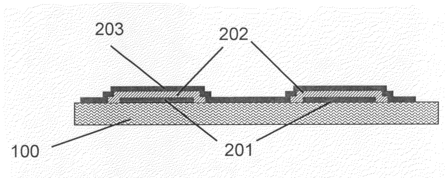
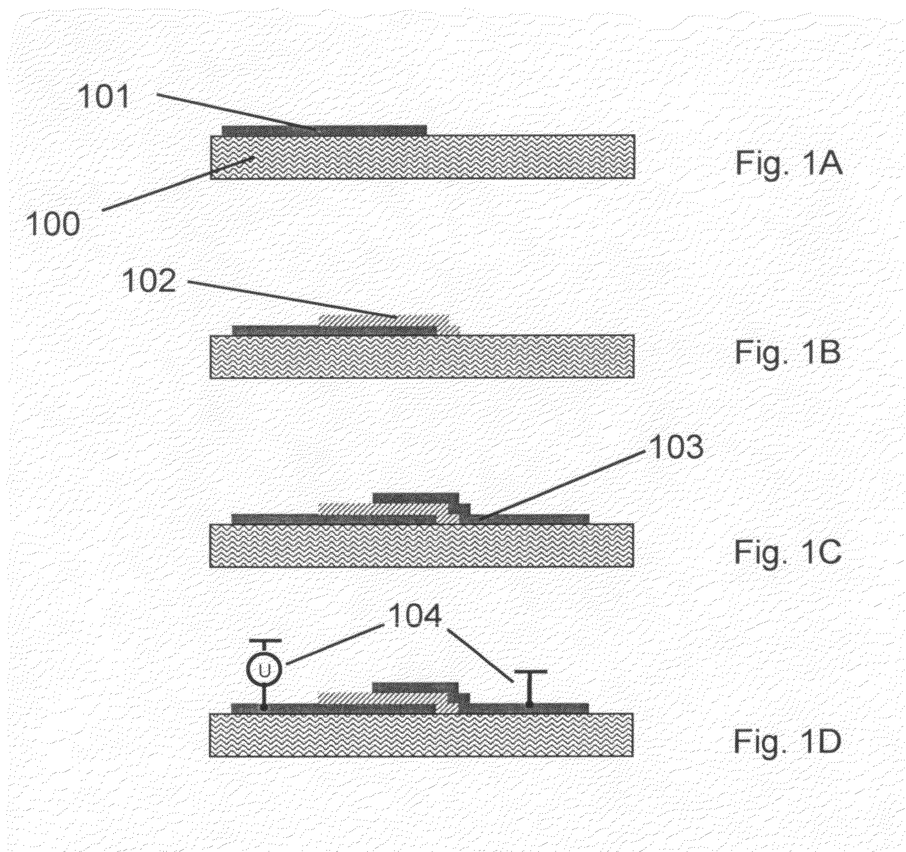
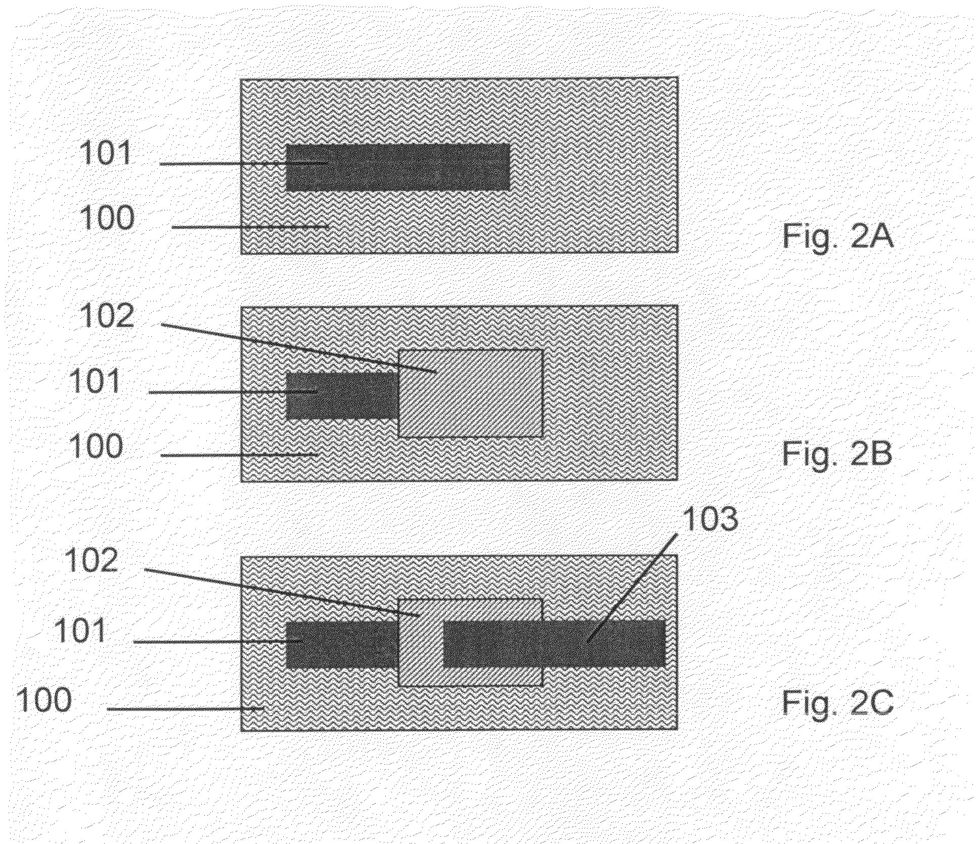
[0063]FIGS. 1 and 2 describe one preferred embodiment of the invention. Here, a vertical parallel-plate three-layer structure is realized that serves as a write-once-read-many (WORM) memory element. The fabrication and operation procedure essentially consist of steps (A) . . . (D) illustrated in FIG. 1. A key property of the structure is that it is made of two nanoparticle inks N1 and N2 that sinter at temperatures Tcure12, respectively. The first electrode 101 is first printed of material N1 on the substrate 100 [FIG. 1A] and dried so that further deposition becomes possible. The middle layer 102 is then printed of material N2 and dried for allowing further deposition [FIG. 1B]. The second electrode 103 is then printed of material Ni and dried [FIG. 1C]. At this point, the entire structure is ready to be sintered at temperature Tcure1cure2, so that the two electrodes 101, 103 become sintered and well-conducting while the middle layer 102 remains unsintered. Such nanoparticle inks s...


PUM

PropertyMeasurementUnit
Timeaaaaaaaaaa
Temperatureaaaaaaaaaa
Electrical conductivityaaaaaaaaaa

Abstract

This publication concerns electronics modules comprising at least one first material zone formed of first material which can be structurally transformed by means of electric interaction in order to increase its conductivity at least locally, the first material having a first transformation threshold, and at least one second material zone in the vicinity of the first material zone. According to the invention, the second material zone is formed from second material, which can also be structurally transformed in order to increase its conductivity, the second material having a second transformation threshold, which is lower than the transformation threshold of the first material zone. With the aid of the invention, post-processing electrical programmability and non-volatility of printable memories can be achieved.

Description

FIELD OF THE INVENTION[0001]The invention concerns electrical units, such as memory devices, in particular printable memories and the fabrication of same. The memories can be utilized, for example, in low-cost RFID, sensor, or media applications. The invention also relates to a method for manufacturing.BACKGROUND OF THE INVENTION[0002]Conductor structures can be created based on metallic nanoparticle suspensions printed on plastic or paper substrates and sintered at plastic / paper-compatible temperatures (T<200° C.). Such silver nanoinks are readily available from companies such as Cabot Inc. or Harima Inc. In addition to sintering at oven, laser [N. Bieri et al., Superlattices and Microstructures 35, 437 (2004).], UV and microwave [J. Perelaer et al., Adv. Mater. 18, 2101 (2006)] sintering is also known in prior art.[0003]Patent Application FI 20060697, still unpublished when filing the present application, describes an improved method for sintering nanoparticle systems, electric...

Claims


Application Information

Patent Timeline
IPC IPC(8): H03H11/40B05D5/12B05D3/14H01S4/00
CPCB82Y10/00Y10T29/49002H01L27/101G11C13/0014H01L21/64G11C11/56G11C17/16H10B63/00
Inventor MATTILA, TOMIALASTALO, ARIALLEN, MARKSEPPA, HEIKKI
Owner VALTION TEKNILLINEN TUTKIMUSKESKUS
Why Eureka
Try Eureka